Waveguide Junction

a technology of waveguides and junctions, applied in the field of waveguide junctions, can solve the problems of increasing manufacturing effort and expense, complex manufacturing of such junctions, and substantial limitations of achievable performance, and achieve the effects of convenient manufacturing, high performance properties, and compact siz

Active Publication Date: 2009-08-13
TELEFON AB LM ERICSSON (PUBL)
View PDF4 Cites 0 Cited by
  • Summary
  • Abstract
  • Description
  • Claims
  • Application Information

AI Technical Summary

Benefits of technology

[0006]Accordingly, the invention seeks to preferably mitigate, alleviate or eliminate one or more of the disadvantages mentioned above singly or in any combination.
[0009]The present invention beneficially allows for interconnecting waveguides that exhibit a linear offset of their central axes and additionally a different angular alignment of their cross sections and provides compact size and easy manufacturing from one solid block of metal. Additional advantage is that high performance properties (extreme low VSWR) over broad frequency bands (up to the determined operating band of standard waveguides with typically 40% bandwidth) are achieved. The junction interfaces exhibit no angular offset to the connecting waveguides and consequently there are no problems with any standard flange interconnections (e.g. in sealed waveguide systems). In addition, the length of the manufactured part can be fitted to overall assembly requirements—it depends no longer on the operating frequency band.

Problems solved by technology

However such a design is only possible for not more than two transformer steps, which yields substantial limitations for the achievable performance (i.e., Voltage Standing Wave Ratio, VSWR, and bandwidth).
Another drawback of the prior art solutions results from the fact, that this solution would commonly exhibit an angular offset at the flange interconnections (interfaces).
Two part format of these junctions allows for more complicated machining and in consequence achieving improved performance, but manufacturing of such junctions is complicated, expensive and time consuming.
If two (or more) parts are used they need to be combined in an appropriate way, which increases the manufacturing effort and expense.
They could be assembled by screws—but such a solution needs additional sealing means in the parting plane if the component is used in a pressurized waveguide system.
Moreover the realization of the component from two (or more) parts yields additional tolerances (e.g., fitting of the parts) that may impair the optimal performance.

Method used


Image

  • Waveguide Junction
  • Waveguide Junction
  • Waveguide Junction

Examples


Embodiment Construction

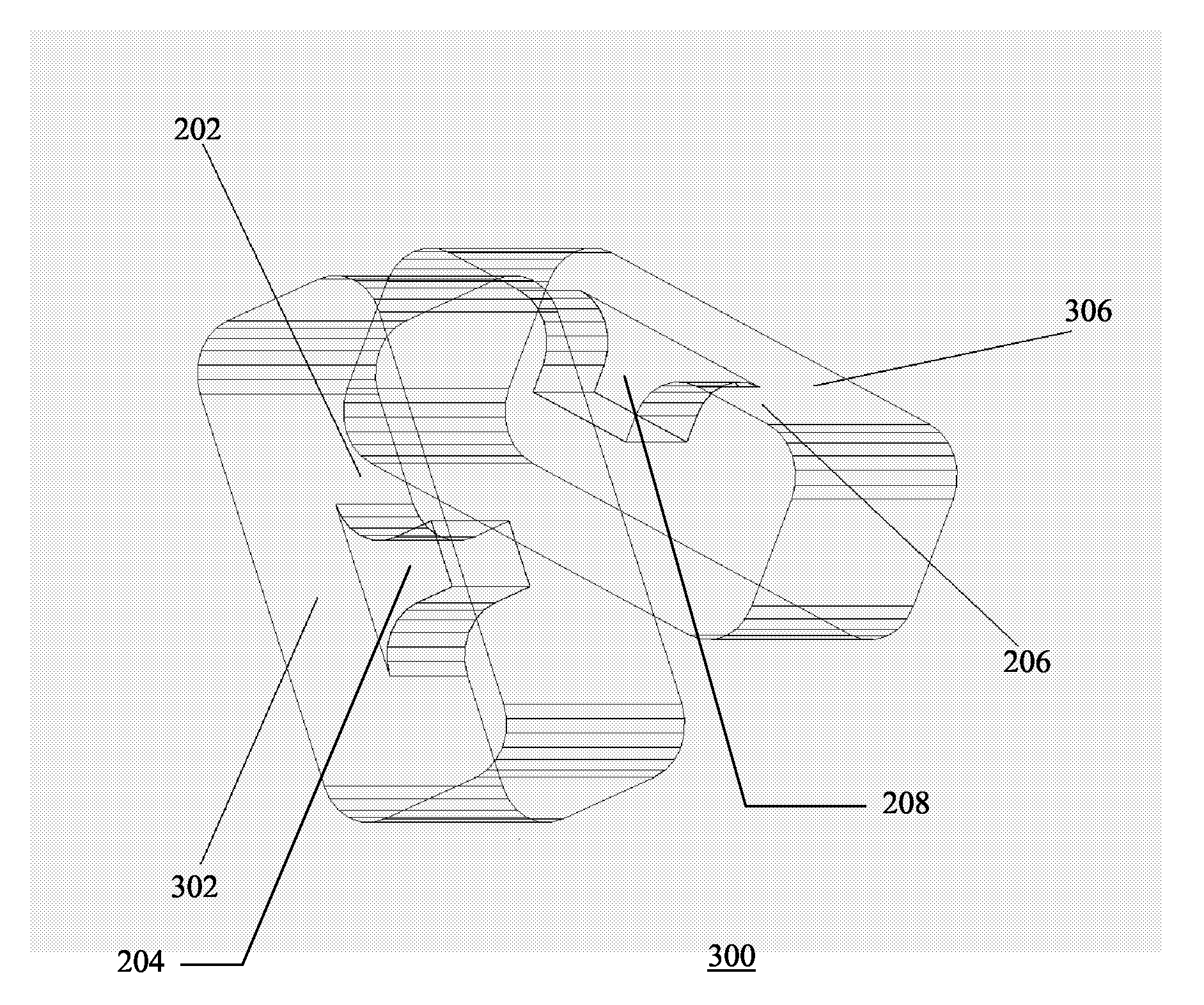
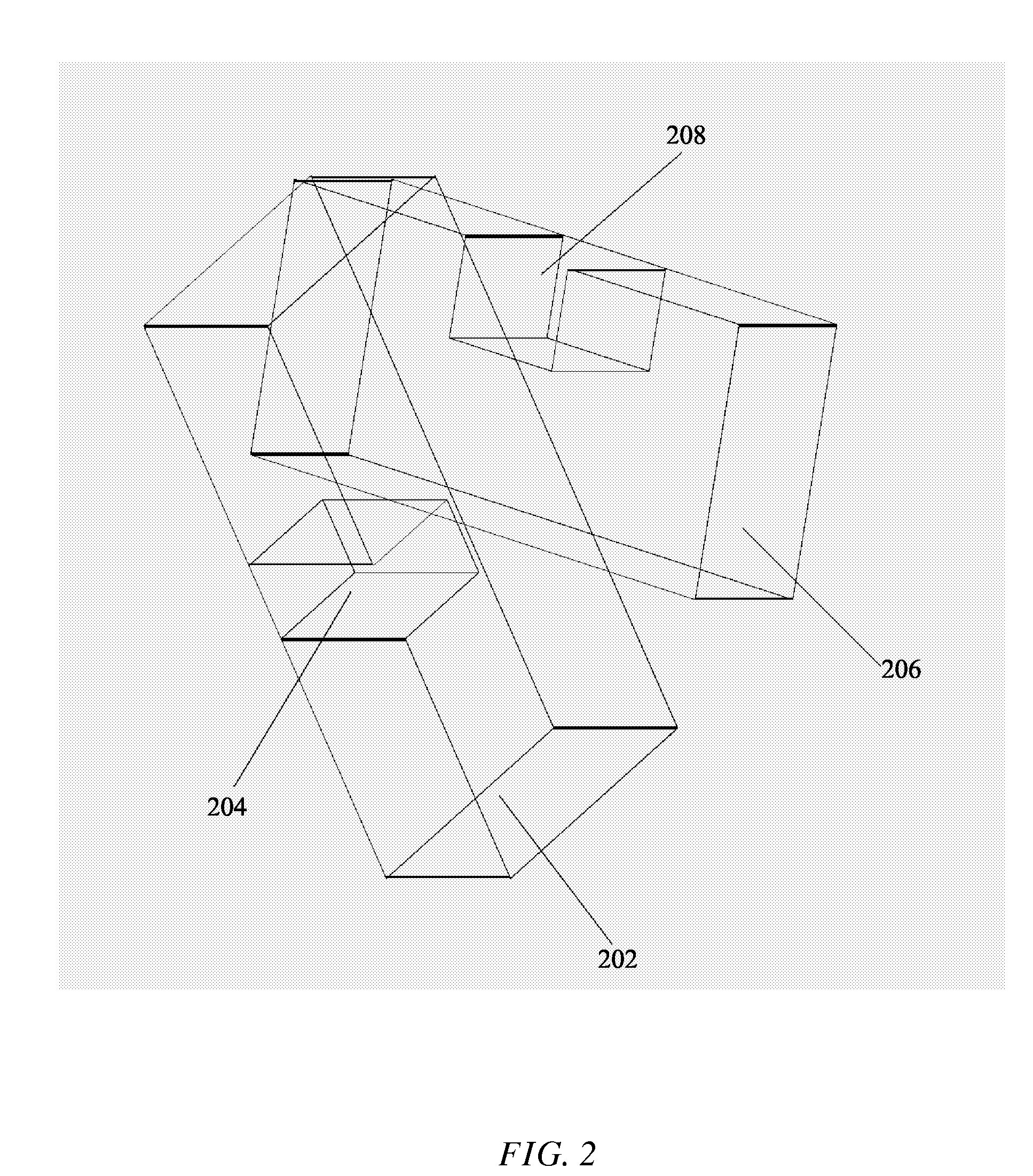
[0015]With reference to FIG. 2 and FIG. 3 a junction 300 for connecting two waveguides is presented. For the sake of clarity the drawings present the invention in a very schematic way with elements and lines not essential for understanding the invention omitted.

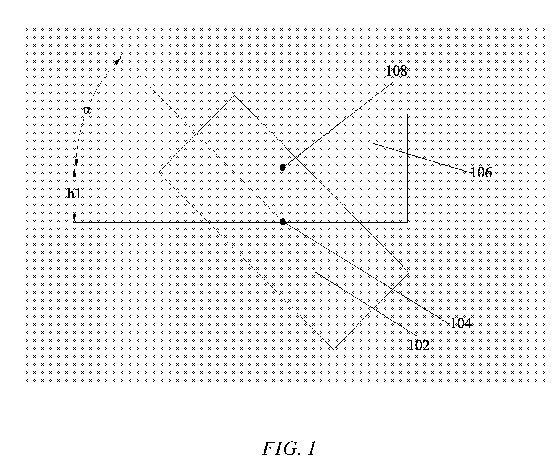
[0016]FIG. 1 shows the cross sections of two waveguides to be interconnected and their cross sections exhibit angular, α, and a first linear offset h1. The interconnection, to be effective, must ensure low reflections in the desired operating frequency band. In the shown example, the center axis of the first waveguide is located at the bottom broad wall of the second waveguide and the cross sections of the waveguides exhibit a 45° angular alignment to each other. In alternative embodiments the angular offset can be also below or above 45° and the linear offset can be such that the center axis of the first waveguide is not located on the broad wall of the second waveguide.

[0017]One embodiment of the novel waveguide twist accor...


PUM


Abstract

A junction (300) for connecting two waveguides having an angular offset between longitudinal symmetry axes of their cross-sections and a first linear offset of the center axes of the waveguides. The junction (300) comprises at least a first and a second transformer sections (202, 206) both having said first angular offset between longitudinal symmetry axes of their cross-sections and said first linear offset of their center axes, wherein each of said transformer sections (202, 206) has one protruded ridge (204, 208) on broad walls, wherein the first ridge (204) is mainly situated outside the cross section of the second transformer section 206 and the second ridge (208) is mainly situated outside the cross section of the first transformer section (202).

Description

FIELD OF THE INVENTION[0001]The present invention relates to a waveguide junction for connecting waveguides having a linear offset of their central axes and, additionally, a different angular alignment of their cross sections.BACKGROUND OF THE INVENTION[0002]Waveguide junctions used to rotate the field orientation for matching two waveguides, which are not aligned are also known as waveguide twists. In solutions known in the art and applicable in situations where the two joined waveguides exhibit an angular offset the vector of the electric field is rotated in intermediate waveguide sections with appropriate angular steps from the input to the output waveguide. Each angular step gives rise to a partial reflection of the wave depending on the angular increment. In a proper design, these partial reflections should cancel at the centre frequency; therefore the length of each section is favourably in the order of a quarter waveguide wavelength (or an odd multiple thereof). The overall b...

Claims


Application Information

Patent Timeline
Patent Type & Authority Applications(United States)
IPC IPC(8): H01P1/165
CPCH01P1/022
Inventor ROSENBERG, UWEMAHR, ULRICH
Owner TELEFON AB LM ERICSSON (PUBL)
Why Eureka
Try Eureka