This helps you quickly interpret patents by identifying the three key elements:
Problems solved by technology
Method used
Benefits of technology
Benefits of technology
[0010]It is an object of the invention to provide a semiconductor light-emitting device with enhanced light-extraction efficiency that light inputted perpendicularly and obliquely to the reflection region can be efficiently extracted from the semiconductor light-emitting device.
Problems solved by technology
Thus, of light emitted from the light-emitting layer, light inputted obliquely to the reflection region is difficult to efficiently extract from the semiconductor light-emitting device.
Method used
Image
Click on the blue label to locate the original text in one second.
Reading with bidirectional positioning of images and text.
Examples
first embodiment
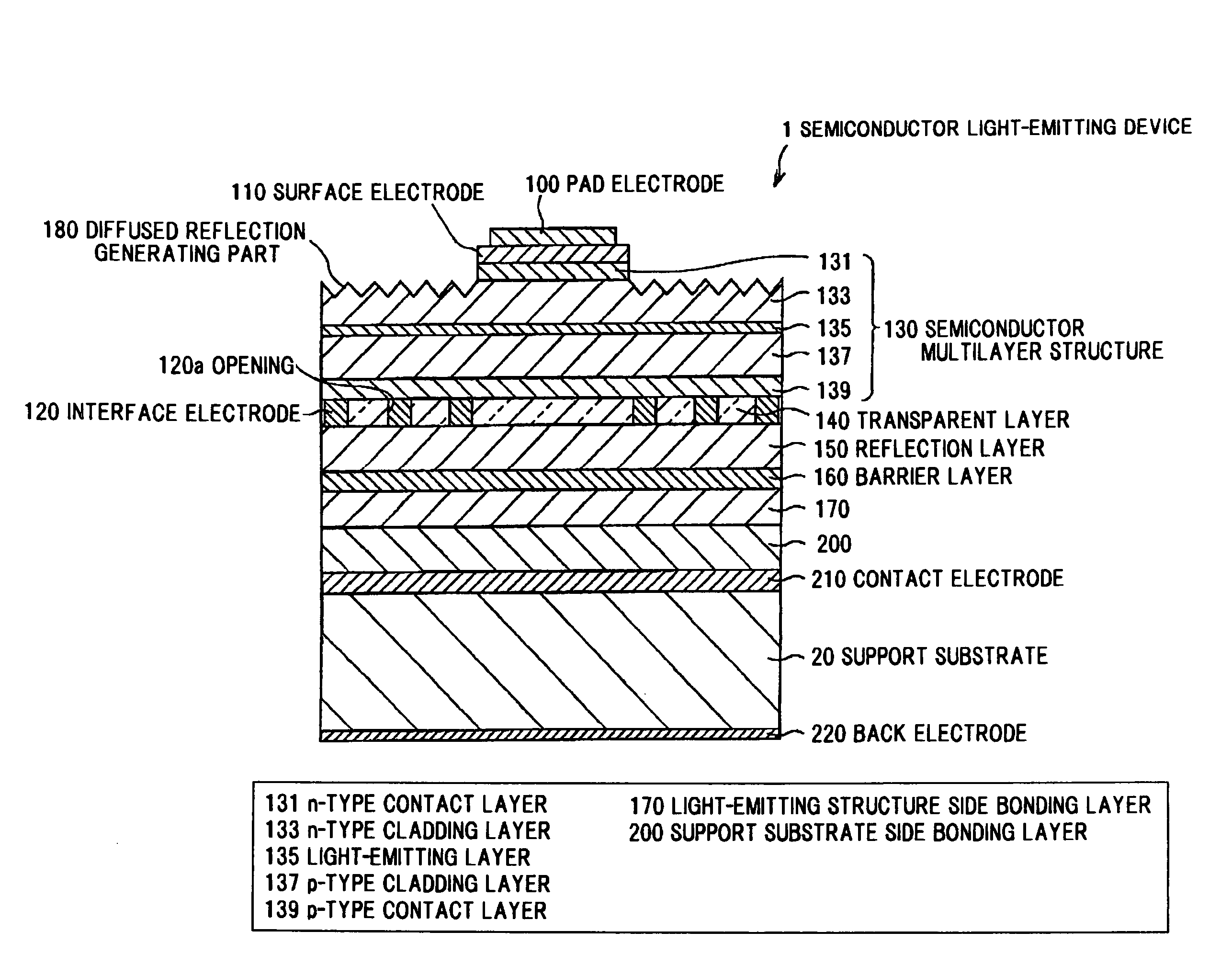
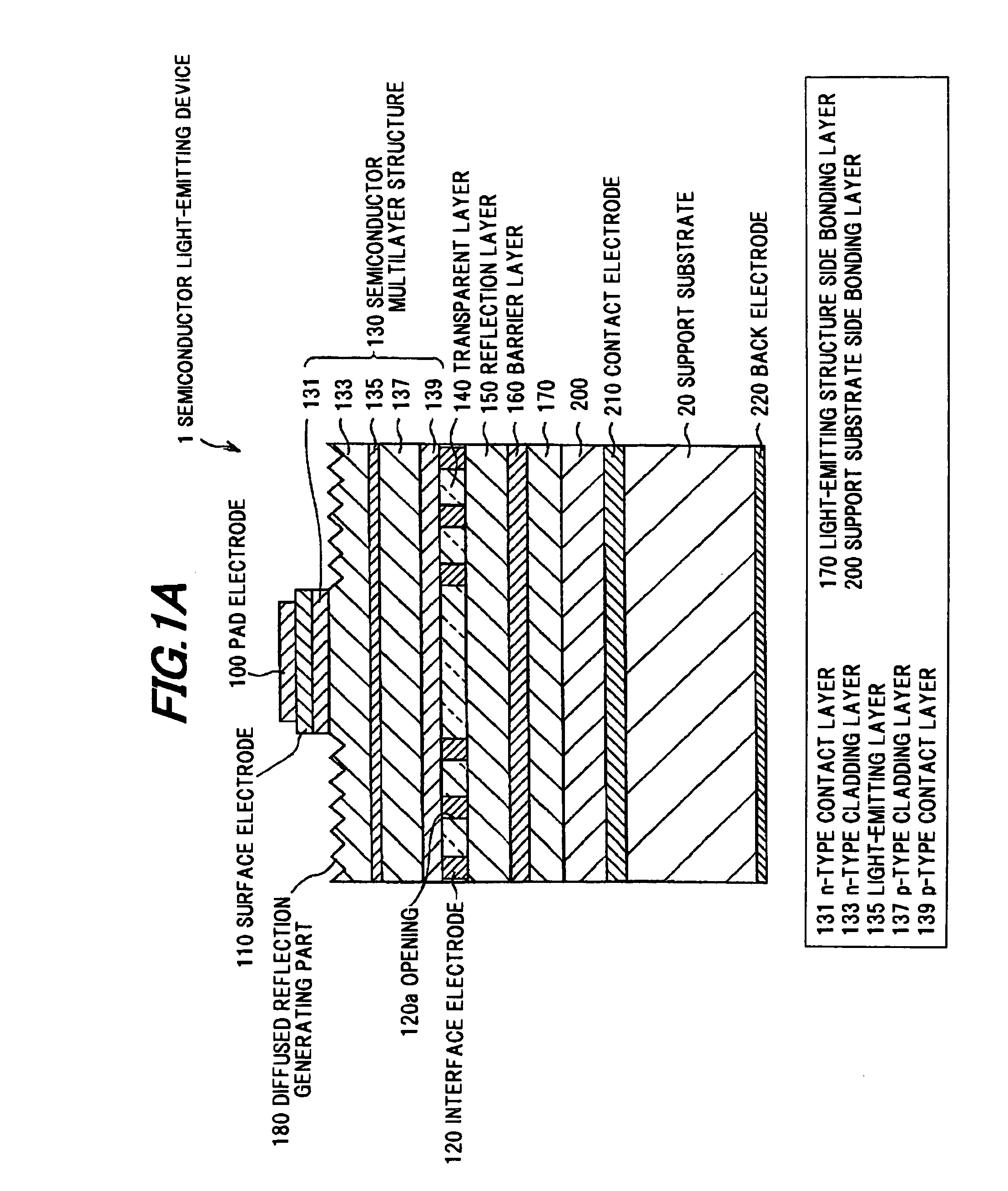
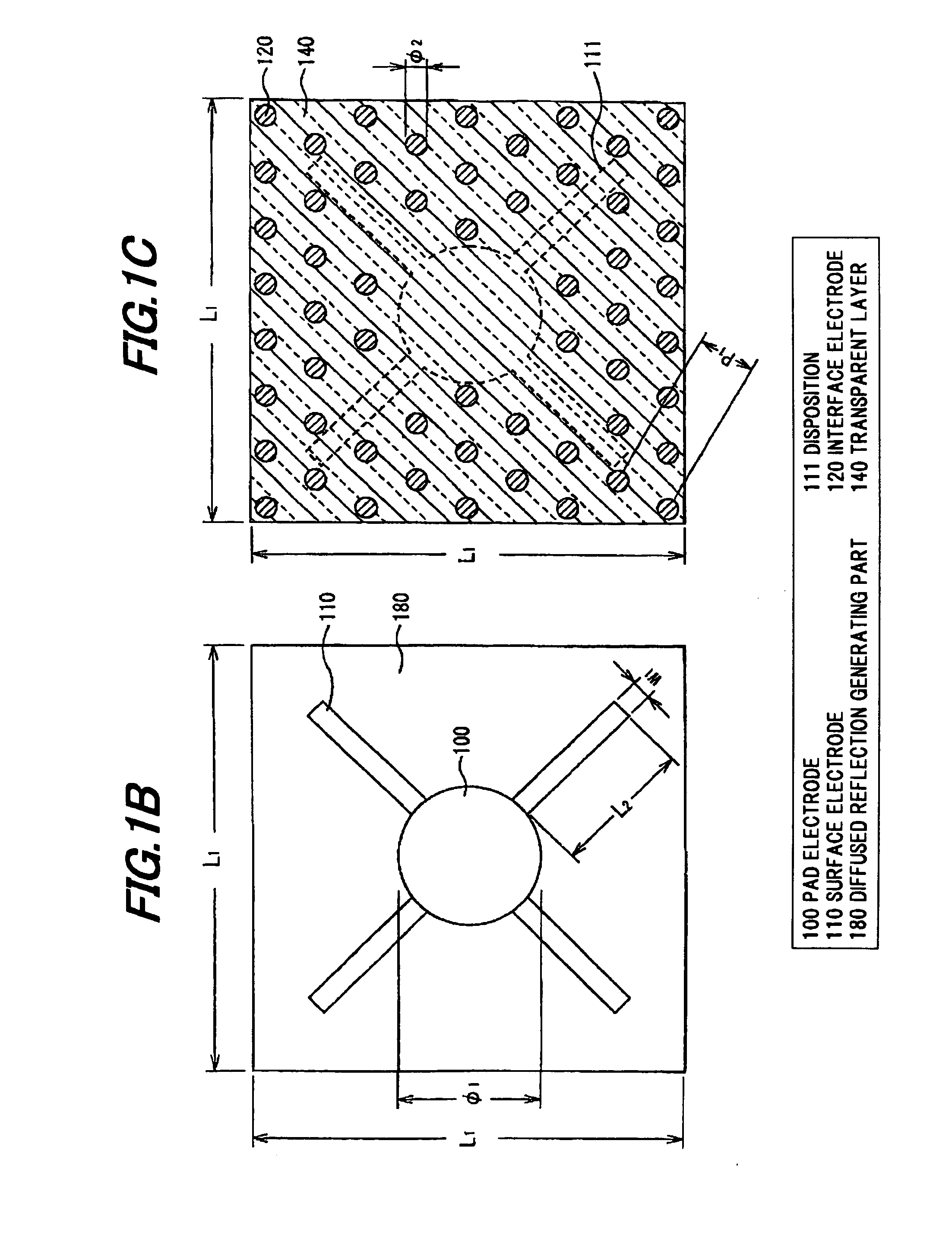
[0049]FIG. 1A is a schematic cross sectional view showing the semiconductor light-emitting device in a first embodiment of the invention. FIG. 1B is a top view showing the semiconductor light-emitting device in the first embodiment, and FIG. 1C is a top cutaway view showing the semiconductor light-emitting device in the first embodiment where the semiconductor light-emitting device is cut away at a transparent layer.
[0050]Structure of Semiconductor Light-Emitting Device 1
[0051]The semiconductor light-emitting device 1 in the first embodiment is composed of a semiconductor multilayer structure 130 including a light-emitting layer 135 as an active layer for emitting light with a predetermined wavelength, a surface electrode 110 electrically connecting with a part of one surface of the semiconductor multilayer structure 130, and a pad electrode 100 disposed on the surface electrode 110 and used for wire bonding.
[0052]The semiconductor light-emitting device 1 is further composed of inte...
second embodiment
[0137]FIG. 5 is a schematic cross sectional view showing a semiconductor light-emitting device in the second embodiment of the invention.
[0138]The semiconductor light-emitting device 1 of the first embodiment is formed to have a top and bottom surface electrode structure wherein electric power is supplied from the side of the pad electrode 100 toward the back electrode 220. On the other hand, a semiconductor light-emitting device 1a of the second embodiment has substantially the same composition as that of the semiconductor light-emitting device 1 of the first embodiment except that a part of a p-type cladding layer 137 of a compound semiconductor layer 130 is exposed, and a p-type electrode is provided on the exposed portion to have a so-called top surface two-electrode structure. Accordingly, the detailed description therefor is omitted excluding different points.
[0139]Structure of Semiconductor Light-Emitting Device 1a
[0140]The semiconductor light-emitting device 1a of the secon...
example 1
[0146]A semiconductor light-emitting device according to Example 1 of the invention is produced in accordance with a method of making the semiconductor light-emitting device 1 as described in the first embodiment of the invention. Specifically, a semiconductor light-emitting device having the following composition is produced as the semiconductor light-emitting device of Example 1.
[0147]Namely, a semiconductor multilayer structure 130a of the semiconductor light-emitting device according to Example 1 is produced from the side of a n-type GaAs substrate (3 inch diameter) being the growth substrate 10 in accordance with a MOVPE method in the following order, i.e. a n-type (Al0.7Ga0.3)0.5In0.5P etching stop layer (Si-doped, 200 nm thickness, 1×10¹⁸ / cm3 carrier concentration), a n-type GaAs contact layer (Si-doped, 100 nm thickness, 1×10¹⁸ / cm3 carrier concentration), a n-type (Al0.7Ga0.3)0.5In0.5P cladding layer (Si-doped, 2000 nm thickness, 1×10¹⁸ / cm3 carrier concentration), an undoped...
PUM
Abstract
A semiconductor light-emitting device includes a support structure, and a light-emitting structure. The support structure includes a support substrate, and a support substrate side bonding layer disposed on one surface of the support substrate. The light-emitting structure includes a light-emitting structure side bonding layer bonded to the support substrate side bonding layer, a reflection region disposed on the support substrate side bonding layer opposite the support substrate, and a semiconductor multilayer structure including a light-emitting layer disposed on the reflection region opposite the light-emitting structure side bonding layer for emitting a light with a predetermined wavelength, and a light-extraction surface disposed on the light-emitting layer opposite the reflection region for reflecting diffusely the light. The reflection region includes a transparent layer of a material with a lower refractive index than that of the semiconductor multilayer structure, and a reflection layer of a metallic material. The transparent layer has such a thickness that interference caused by multiple reflection of light inputted to the transparent layer can be suppressed.
Description
[0001]The present application is based on Japanese patent application No. 2008-039271 filed on Feb. 20, 2008, the entire contents of which are incorporated herein by reference.BACKGROUND OF THE INVENTION[0002]1. Field of the Invention[0003]The invention relates to a semiconductor light-emitting device with enhanced light-extraction efficiency.[0004]2. Description of the Related Art[0005]A conventional semiconductor light-emitting device (e.g., see JP-A-2005-513787) with improved light-extraction efficiency is known that is composed of a conductive holder, a semiconductor multilayer structure having multiple semiconductor layers including a light-emitting layer, a reflection layer of a metal and plural interface electrodes and formed on the conductive holder through a transparent layer having a thickness d of λ / (4n), and a surface electrode formed on the semiconductor multilayer structure, where the interface electrodes are formed in an area except under the surface electrode. Meanwh...
Claims
Application Information
Patent Timeline
Application Date:The date an application was filed.
Publication Date:The date a patent or application was officially published.
First Publication Date:The earliest publication date of a patent with the same application number.
Issue Date:Publication date of the patent grant document.
PCT Entry Date:The Entry date of PCT National Phase.
Estimated Expiry Date:The statutory expiry date of a patent right according to the Patent Law, and it is the longest term of protection that the patent right can achieve without the termination of the patent right due to other reasons(Term extension factor has been taken into account ).
Invalid Date:Actual expiry date is based on effective date or publication date of legal transaction data of invalid patent.

