

Organic light emitting diode display device
- Summary
- Abstract
- Description
- Claims
- Application Information
AI Technical Summary
Benefits of technology
Problems solved by technology
Method used
Image

Examples
first embodiment
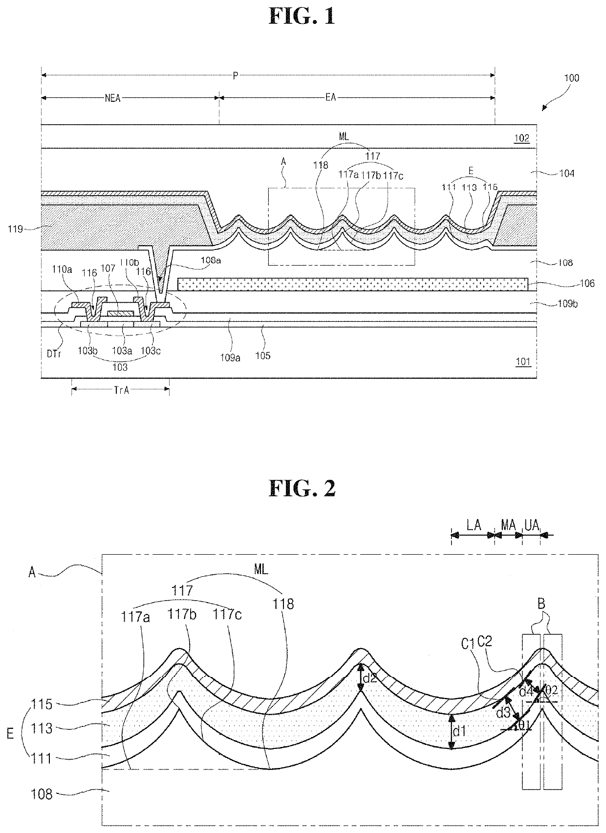
[0022]FIG. 1 is a cross-sectional view showing an organic light emitting diode display device according to the present disclosure. All the components of the organic light emitting diode display devices according to all embodiments of the present disclosure are operatively coupled and configured.
[0023]In FIG. 1, an organic light emitting diode (OLED) display device 100 can have a top emission type or a bottom emission type according to an emission direction of a light. A bottom emission type OLED display device can be exemplarily illustrated hereinafter. All of elements of the organic light emitting diode (OLED) display device 100 are operatively coupled and configured.
[0024]The OLED display device 100 includes a substrate having a driving thin film transistor (TFT) DTr and a light emitting diode E thereon and a protecting film 102 encapsulating the substrate 101.
[0025]The substrate 101 includes a plurality of pixel regions P and each pixel region P includes an emitting area EA where...
second embodiment
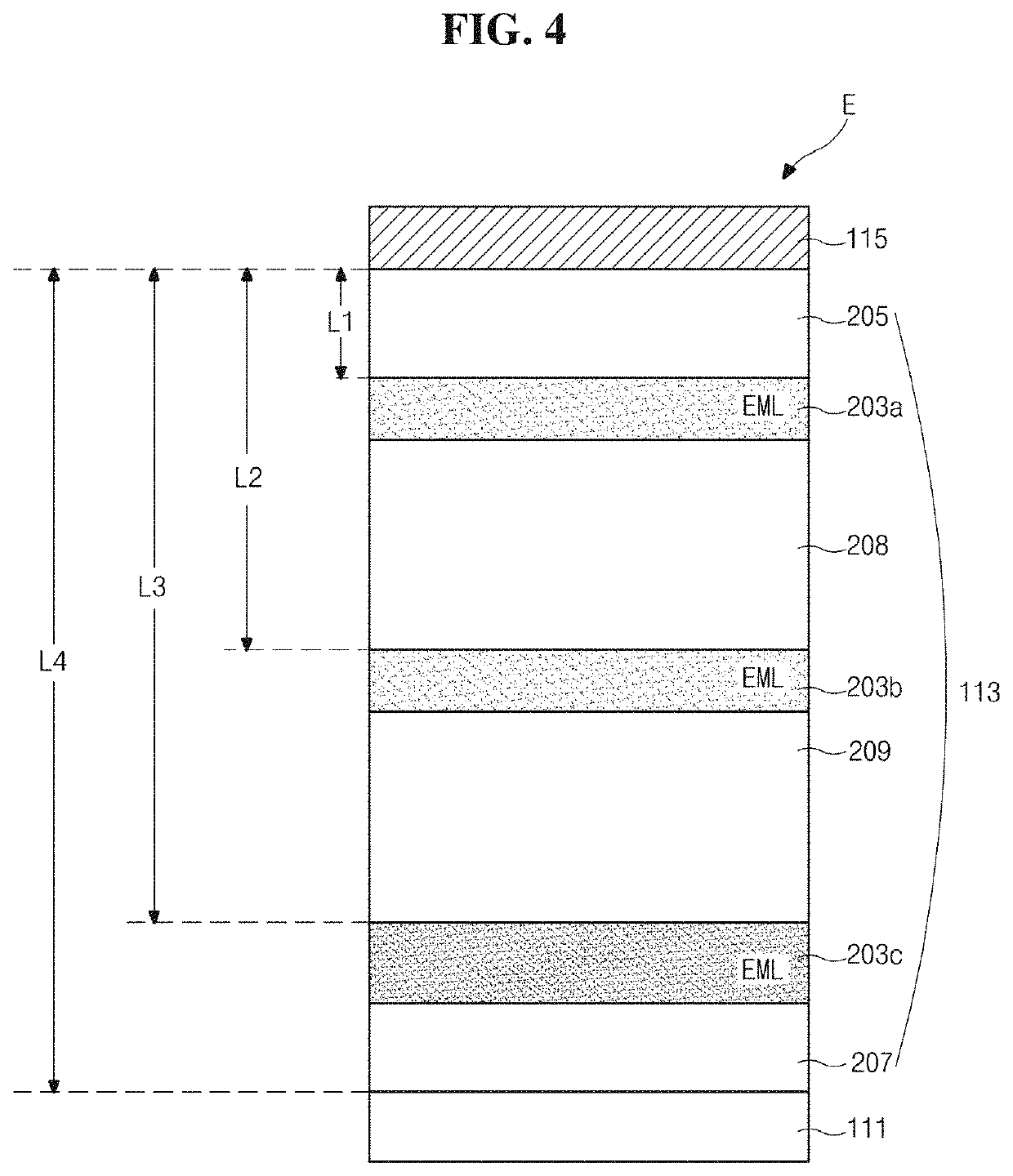
[0107]In a light emitting diode E (of FIG. 1) of an organic light emitting diode (OLED) display device 100 (of FIG. 1) according to the present disclosure, the maximum emission efficiency is obtained and a total thickness of the light emitting diode E is reduced by disposing first, second and third emitting material layers emitting blue, blue and yellow-green colored lights, respectively, sequentially under a second electrode 115 (of FIG. 1) to satisfy cavity peaks. As a result, the maximum emission efficiency is obtained and a total thickness of the light emitting diode E is reduced.
[0108]In FIG. 4, a light emitting diode E includes first and second electrodes 111 and 115 and a light emitting layer 113 between the first and second electrodes 111 and 115, and the light emitting layer 113 includes first, second and third emitting material layers (EMLs) 203a, 203b and 203c and first and second auxiliary layers 208 and 209 among the first, second and third emitting material layers (EML...
PUM
 Abstract
Description
Claims
Application Information