

Semiconductor light-emitting device and method for manufacturing the same
- Summary
- Abstract
- Description
- Claims
- Application Information
AI Technical Summary
Benefits of technology
Problems solved by technology
Method used
Image

Examples
examples
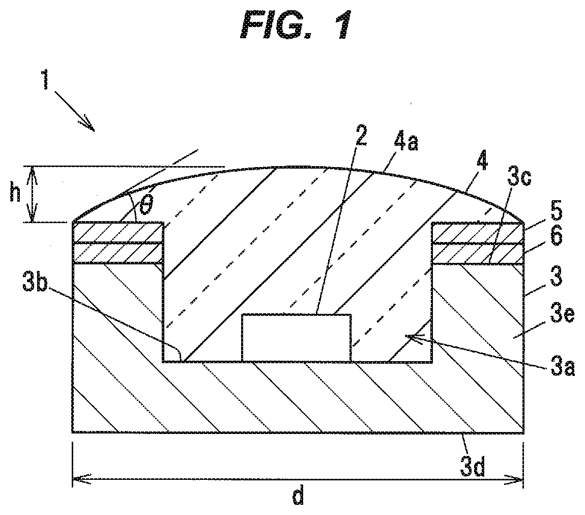
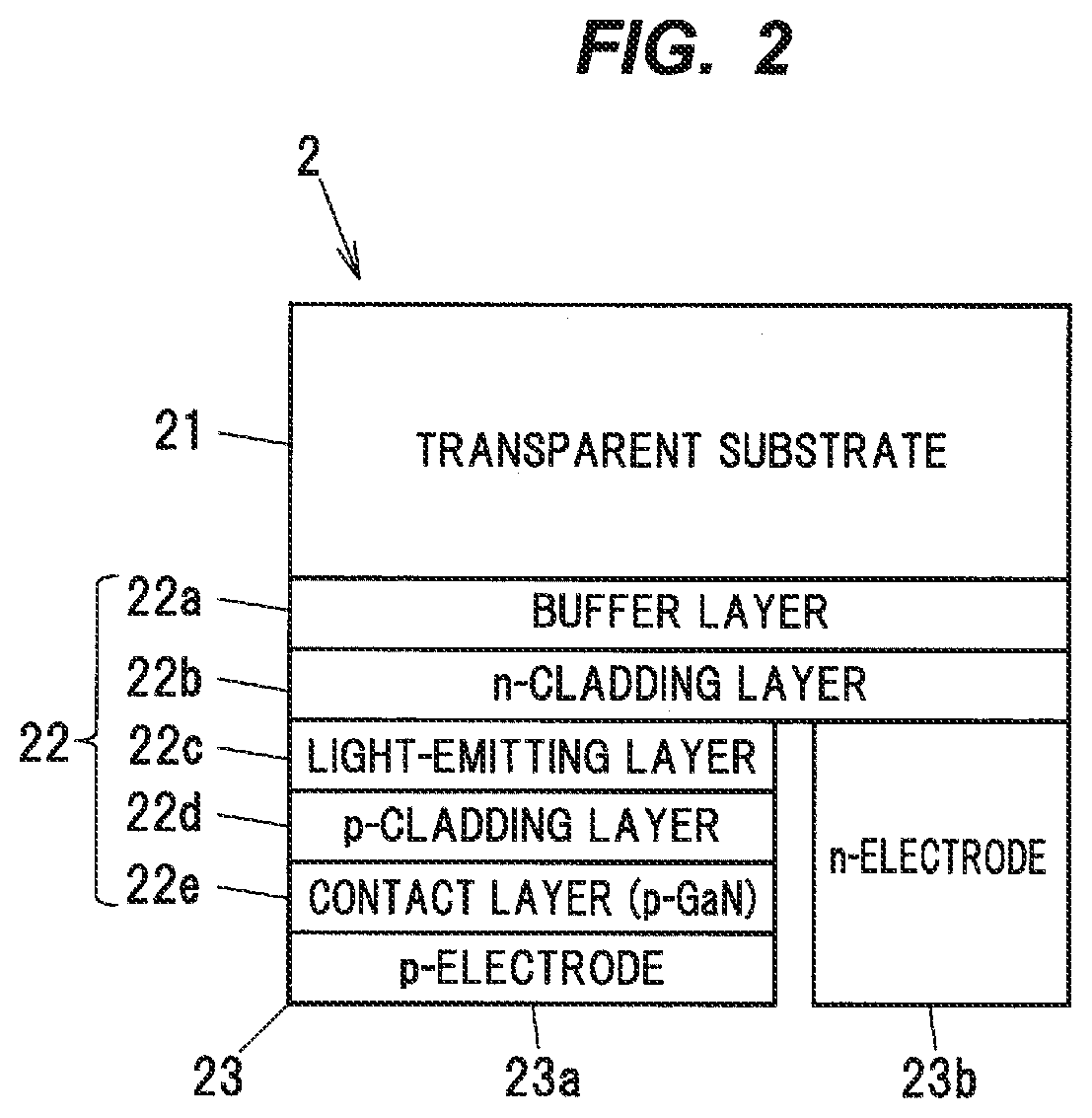
[0073]The light-emitting devices 1 described above were made using the light-emitting element 2 having an emission wavelength 310 nm and a light output of about 60 mW at a current of 350 mA. Meanwhile, a light-emitting device having the sealing material 4 with the flat upper surface 4a as shown in FIG. 4 was prepared as Comparative Example. In the present Examples, the thin film layer 5 was formed of 1 μm-thick gold (Au), and the adhesive layer 6 bonding the rim face 3c of the package substrate 3 to the lower surface of the thin film layer 5 was formed of tungsten (W) (thickness not specified) formed on the rim face 3c of the package substrate 3 and 1 μm-thick nickel (Ni) further formed thereon to improve adhesion of the thin film layer 5.
[0074]Light output of about 75 mW was obtained from the light-emitting device 1 with the contact angle θ of about 15° (hereinafter, also referred to as “Example 1”). That is, in Example 1, light output was improved about 1.25 times. Meanwhile, ligh...
PUM
 Abstract
Description
Claims
Application Information