Method and system for improved testing of transistor arrays

a transistor array and array technology, applied in the field of improved testing of transistor arrays, can solve the problems of difficulty in determining defects before applying display media or before the array is fully fabricated, implementation or impracticality of use, and/or impracticality,

Inactive Publication Date: 2009-09-03
PALO ALTO RES CENT INC
View PDF2 Cites 18 Cited by
  • Summary
  • Abstract
  • Description
  • Claims
  • Application Information

AI Technical Summary

Benefits of technology

[0006]The presently described embodiments comprise, in at least one form, a set of driving electronics, detector electronics, and algorithms to measure performance of active-matrix arrays without making direct pixel-by-pixel contact to the interior of the array....

Problems solved by technology

Finished displays may be characterized by human eye or by camera to detect gross defects, but it has heretofore been difficult and/or impractical to determine defects before applying the display medium or before the array is fully fabricated.
This difficulty increases the cost of the process because defective arrays may be packaged and enter the marketplace.
Notwithstanding the difficulty in implementation or impracticality of use, large area electronic testers have been employed to test active matrix arrays.
However, this type of tester is...

Method used


Image

  • Method and system for improved testing of transistor arrays
  • Method and system for improved testing of transistor arrays
  • Method and system for improved testing of transistor arrays

Examples


Embodiment Construction

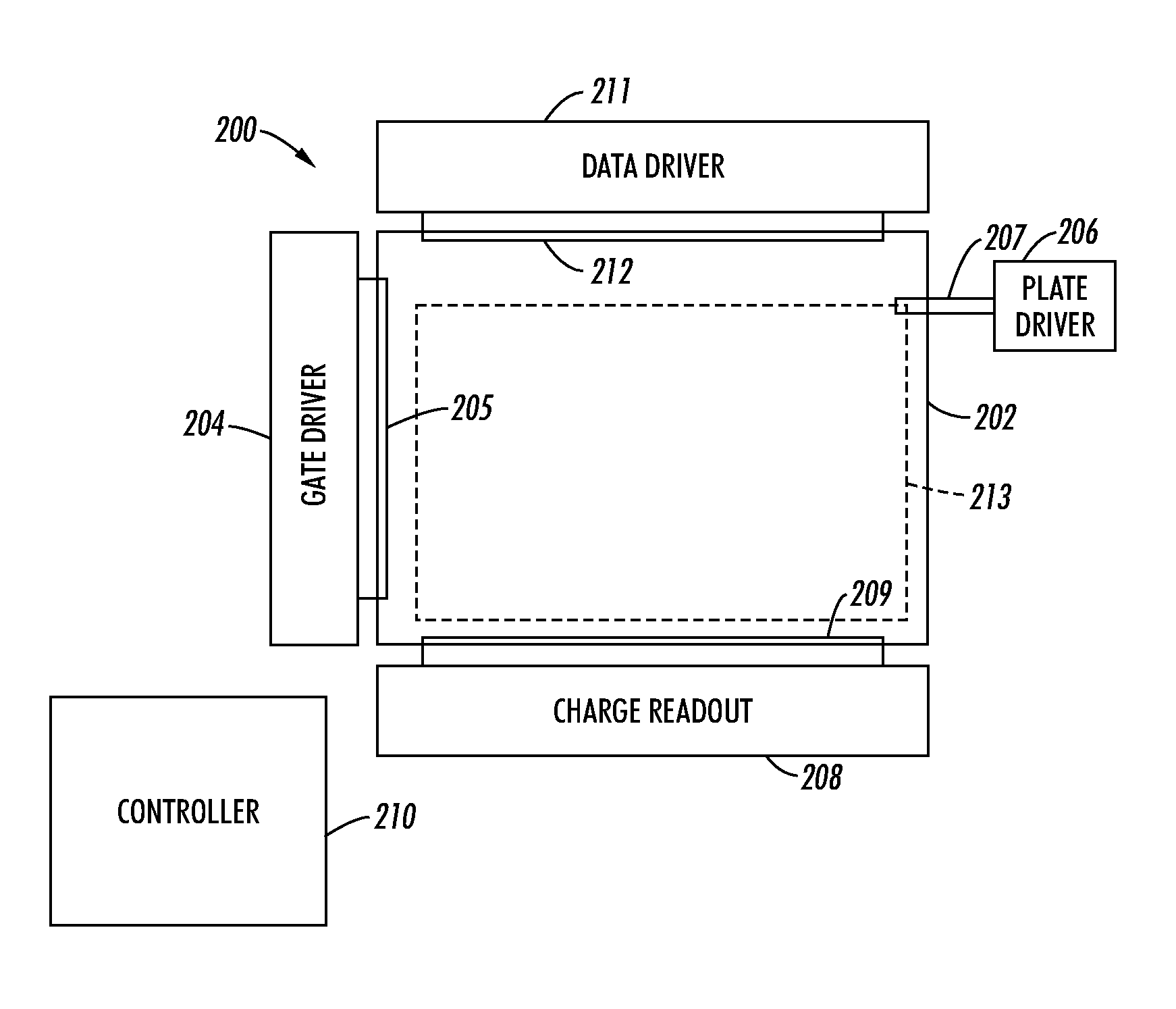
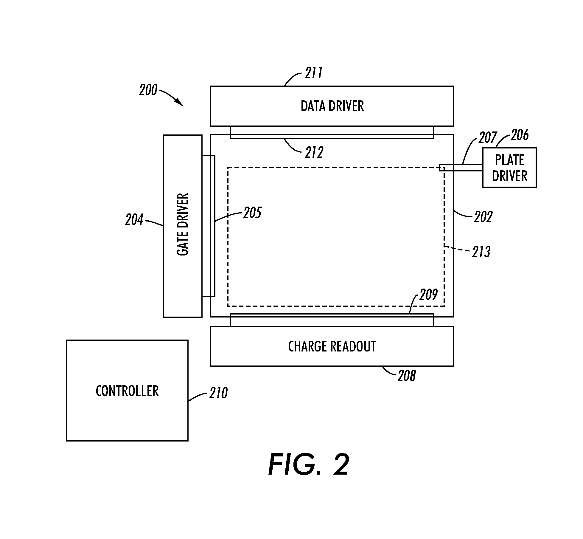
[0056]The presently described embodiments provide a method and a system for testing active matrix arrays such as liquid crystal displays, focal-plane image sensors, light-emitting displays, and electric paper. The techniques according to the presently described embodiments allow for testing of each pixel or transistor of the active matrix before liquid crystals or other media are applied to the active matrix and before the production of the system is complete. This allows for an early detection testing system that is conducive to high production environments.

[0057]Charge sensitive amplifiers and selected voltage drivers (and other mechanisms) may be used (as injecting elements) in conjunction with variable timing and voltages to determine individual pixel or transistor properties over an entire array in just a few seconds. For example, a capacitive elastomer laminate (or plate) or gate lines of selected transistors may be used to inject charge into pixels or transistors. Connection ...


PUM


Abstract

An electronic test system to evaluate the pixel and array properties of active-matrix displays that use charge or current sensitive circuits attached to the array data lines is described. Leakage-current, charging time, and other metrics can be measured for all pixels in the array without electrical or optical connection to the interior of the array. In accordance with the presently described embodiments, charge or current sensitive amplifiers and selected voltage drivers may be used in conjunction with variable timing and voltages to determine individual transistor properties over an entire array in just a few seconds. Signals to be measured may be injected in several ways: first, a capacitive elastomer laminate (or plate) may be applied to the surface of the array, making a capacitance with the pixel pad; second, gate lines may be used to inject charge into pixels that connect to more than one gate line; third, digital or analog drivers connected to the data lines may be used to charge the pixel to varying states; fourth, the dc-bias level of the charge or current sensitive readout electronics may be shifted relative to the gate voltages to charge the pixel. Connection in the system between components is achieved through flex connectors or other appropriate means. Ultimately, an output signal for each pixel is measured. Thus, based on the output signal, the charging time or current, the leakage time or current, and other pixel or transistor parameters may be characterized for the entire array.

Description

BACKGROUND[0001]Active matrix arrays, used for applications such as liquid crystal displays, are typically produced based on very strict criteria. Finished displays may be characterized by human eye or by camera to detect gross defects, but it has heretofore been difficult and / or impractical to determine defects before applying the display medium or before the array is fully fabricated. This difficulty increases the cost of the process because defective arrays may be packaged and enter the marketplace.[0002]Notwithstanding the difficulty in implementation or impracticality of use, large area electronic testers have been employed to test active matrix arrays. Pixel defects, line defects, and area (Mura) defects may be detected on display glass before the shorting bars are removed or the liquid crystal (LC) cell is constructed. Several types of these testers are in use.[0003]For example, an 11,520 pin tester with multiple heads is known. Pin testing allows complete curve tracing of tr...

Claims


Application Information

Patent Timeline
IPC IPC(8): H01H31/02
CPCG09G3/006
Inventor APTE, RAJ B.
Owner PALO ALTO RES CENT INC
Why Eureka
Try Eureka