Top Gate Thin Film Transistor with Enhanced Off Current Suppression

Inactive Publication Date: 2009-09-10
SHARP LAB OF AMERICA INC
View PDF4 Cites 15 Cited by
  • Summary
  • Abstract
  • Description
  • Claims
  • Application Information

AI Technical Summary

Benefits of technology

[0012]Additional details of the above-described method and a bottom-contac

Problems solved by technology

However, the above-described channel contact structure is not necessarily optimal for use with mid-mobility active layers made from μc-Si.
Alternately stated, the simplicity of conventional structure and processes puts cons

Method used


Image

  • Top Gate Thin Film Transistor with Enhanced Off Current Suppression
  • Top Gate Thin Film Transistor with Enhanced Off Current Suppression
  • Top Gate Thin Film Transistor with Enhanced Off Current Suppression

Examples


Embodiment Construction

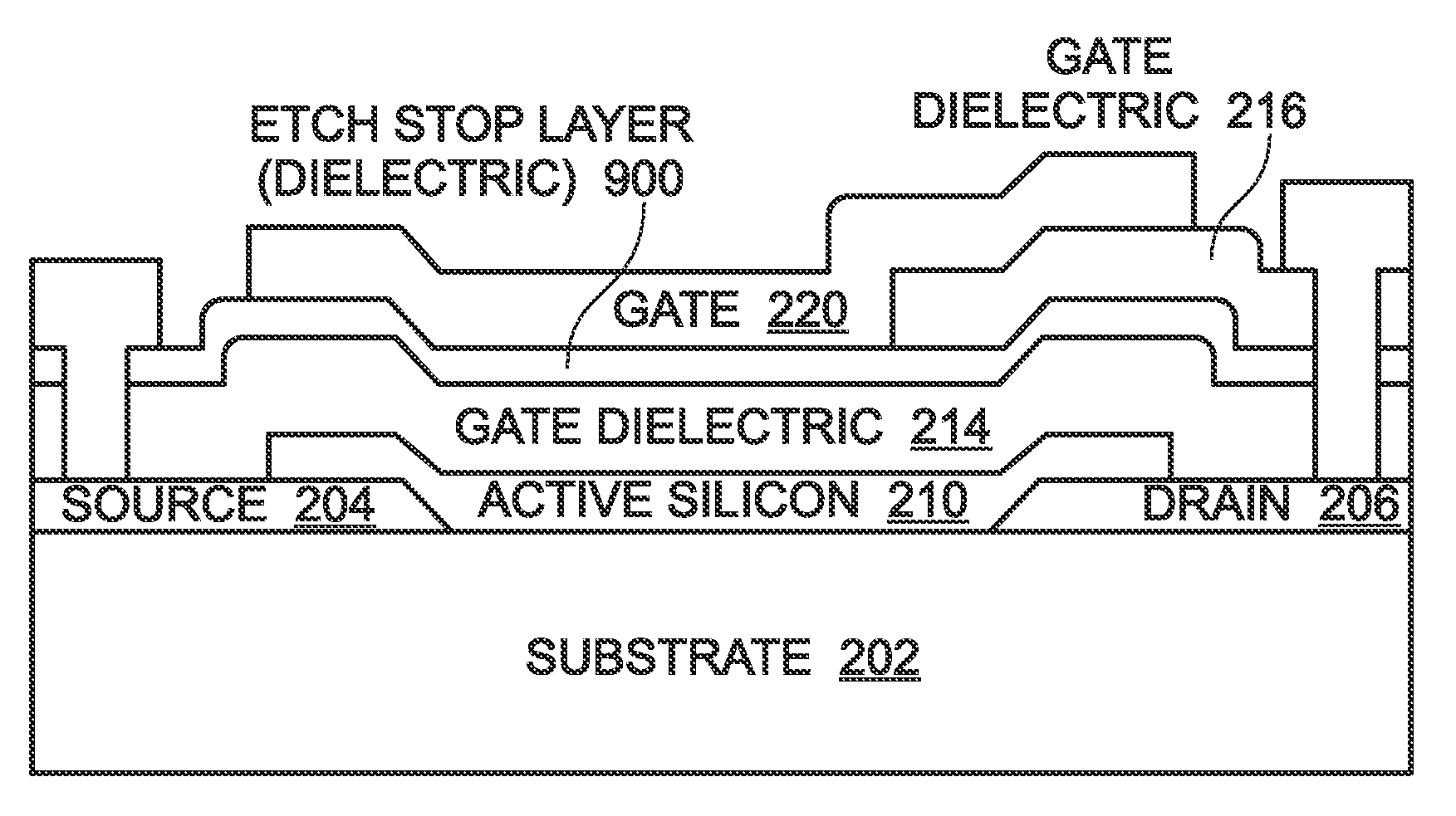
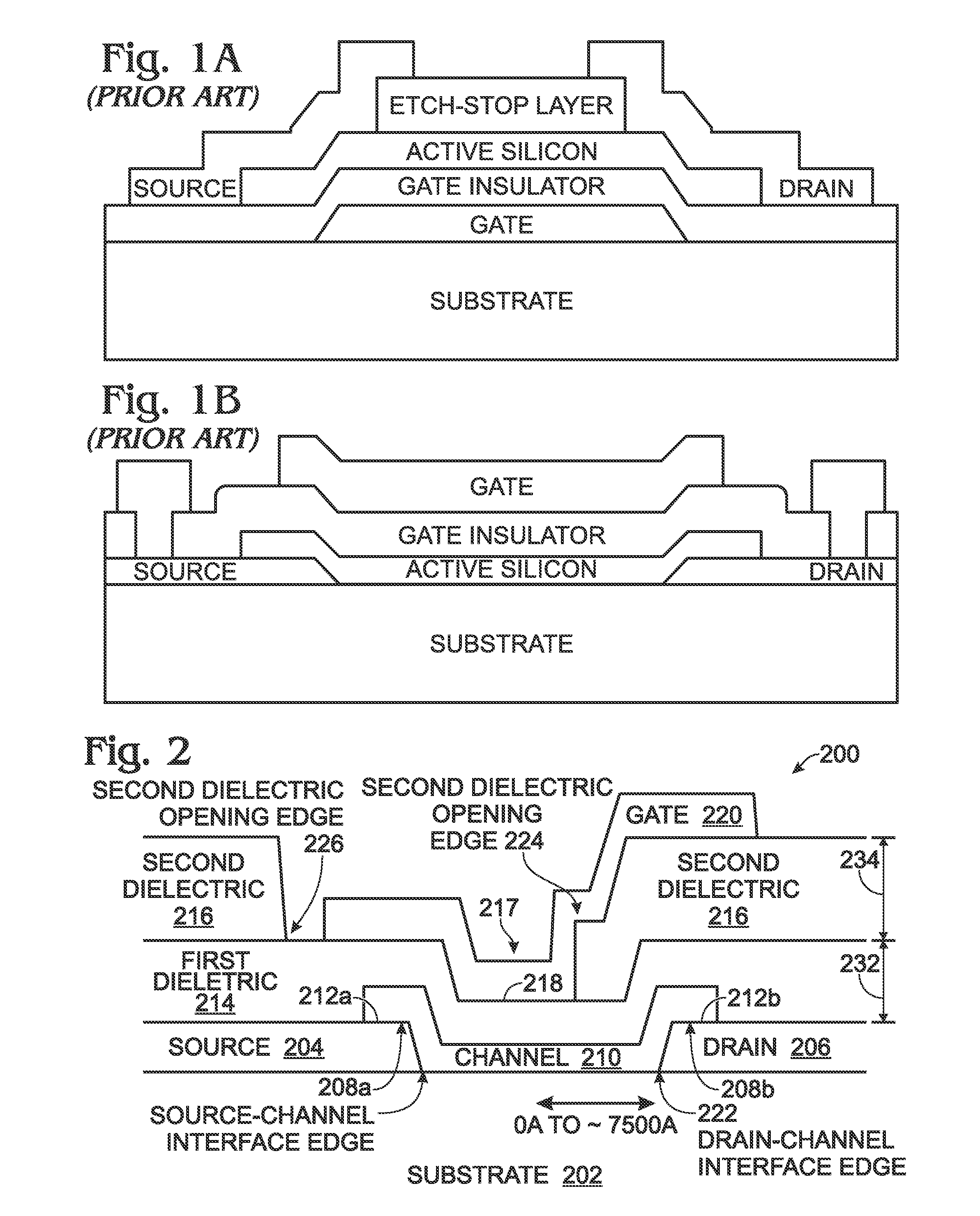
[0021]FIG. 2 is a partial cross-sectional view of a bottom-contacted top gate thin film transistor (TFT) with enhanced off current suppression. The TFT 200 comprises a substrate 202, which may be a material such as metal foil, Si, glass, plastic, or quartz. However, other unnamed substrate materials may also be used that are well known in the art. A source region 204 and a drain region 206 overlie the substrate 202, each having a channel interface top surface 208a and 208b, respectively. A channel 210 interposed between the source 204 and drain 206, with contact regions 212a and 212b, respectively, immediately overlying the source / drain (S / D) interface top surfaces 208a and 208b.

[0022]A first dielectric layer 214 overlies the channel 210, source 204, and drain 206. A second dielectric layer 216 overlies the S / D interface top surfaces 208, with an opening 217 exposing a portion 218 of the first dielectric 214 overlying the channel 210. A gate 220 overlies the second dielectric layer...


PUM


Abstract

A bottom-contacted top gate thin film transistor (TFT) with enhanced off current suppression is provided, along with an associated fabrication method. The method provided a substrate. Source and drain regions are formed overlying the substrate, each having a channel interface top surface. A channel is interposed between the source and drain, with contact regions immediately overlying the source/drain (S/D) interface top surfaces. A first dielectric layer is conformally deposited. Then, a second dielectric layer is formed overlying the S/D interface top surfaces, with an opening exposing a portion of the first dielectric overlying the channel. A gate is formed overlying the second dielectric layer and the exposed portion of the first dielectric layer.

Description

BACKGROUND OF THE INVENTION[0001]1. Field of the Invention[0002]This invention generally relates to integrated circuit (IC) fabrication and, more particularly, to a gate dielectric structure that permits enhanced off current suppression in a top gate thin-film transistor (TFT).[0003]2. Description of the Related Art[0004]FIGS. 1A and 1B are, respectively, partial cross-sectional views of bottom gate and top gate TFT devices made using an amorphous silicon (Si) active layer (prior art). For ease of fabrication using well-established process flows, the channel is formed from a thin-film material that is interposed between the source and drain, while overlapping the regions (contact regions) of the source and drain. Such a structure is optimal for amorphous Si (a-Si) active layer because the gate / contact overlap ensures low contact resistance without causing high off current.[0005]To economically fabricate higher quality consumer devices such a liquid crystal display (LCD) televisions,...

Claims


Application Information

Patent Timeline
IPC IPC(8): H01L29/786H01L21/335
CPCH01L29/42384H01L29/78609H01L29/66757
Inventor KISDARJONO, HIDAYATVOUTSAS, APOSTOLOS T.
Owner SHARP LAB OF AMERICA INC
Why Eureka
Try Eureka