Semiconductor Memory Device and Method for Arranging and Manufacturing the Same

a memory device and semiconductor technology, applied in semiconductor devices, digital storage, instruments, etc., can solve the problems of large chip size and increased area siz

Inactive Publication Date: 2009-09-10
SAMSUNG ELECTRONICS CO LTD
View PDF25 Cites 152 Cited by
  • Summary
  • Abstract
  • Description
  • Claims
  • Application Information

AI Technical Summary

Benefits of technology

[0028]The first to fourth pull-up transistors are PMOS transistors, and the first to third pull-down transistors are NMOS transistors. A transistor to be arranged on a first layer is a bulk transistor, and a transistor to be arranged on a second or more layer is a thin film transistor.
[0029]A transistor to be arranged on the first layer among the at least two layers of the peripheral circuit is one which is possible to be arranged together with...

Problems solved by technology

Thus, as the capacity of the memory cell array (i.e., the number of the memory cells...

Method used


Image

  • Semiconductor Memory Device and Method for Arranging and Manufacturing the Same
  • Semiconductor Memory Device and Method for Arranging and Manufacturing the Same
  • Semiconductor Memory Device and Method for Arranging and Manufacturing the Same

Examples


first embodiment

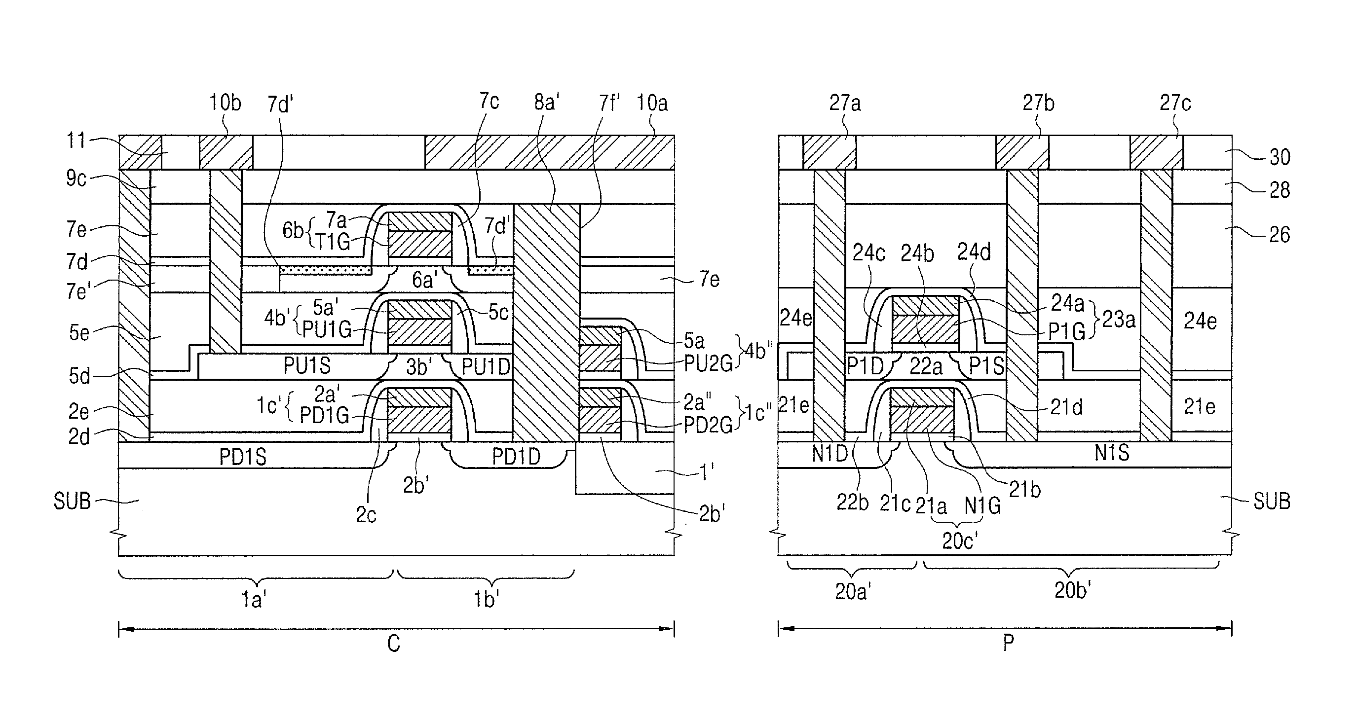
[0083]FIGS. 7A to 7D are views respectively illustrating arrangement of transistors of a static memory cell and transistors which constitute an inverter, a NAND gate and a NOR gate of a peripheral circuit of a semiconductor memory device according to the present invention. In particular, FIGS. 7A to 7D show arrangement of transistors which constitute the peripheral circuit in case where transistors which constitute the memory cell are arranged on two layers.

[0084]Like arrangement of FIG. 5A, transistors PD1, PD2, PU1, PU2, T1, and T2 of FIG. 7A that constitute the static memory cell are arranged on two layers. As shown in FIG. 7B, an NMOS transistors N1 is arranged on the first layer 1F, and a PMOS transistor P1 is arranged on the second layer 2F. Connection between the transistors N1 and P1, which constitute the inverter, are identical to those of FIG. 4B. As shown in FIG. 7C, NMOS transistors N2 and N3 are arranged on the first layer 1F, and PMOS transistors P2 and P3 are arranged...

second embodiment

[0086]FIGS. 8A to 8D are views respectively illustrating arrangement of transistors of a static memory cell and transistors which constitute an inverter, a NAND gate and a NOR gate of a peripheral circuit of a semiconductor memory device according to the present invention. In particular, FIGS. 8A to 8D show arrangement of transistors which constitute the peripheral circuit in case where transistors which constitute the memory cell are arranged on three layers. Like arrangement of FIG. 6A, the transistors of FIG. 8A, which constitute the static memory cell, are arranged such that the pull-down transistors PD1 and PD2 are arranged on the first layer 1F, the pull-up transistors PU1 and PU2 are arranged on the second layer 2F, and the transmission transistors T1 and T2 are arranged on the third layer. As shown in FIG. 8B, NMOS transistors N1-1 and N1-2, which have 1 / 2 channel width of channel width of the NMOS transistor N1 of FIG. 3B are arranged. The NMOS transistor N1-2 is arranged o...

third embodiment

[0090]FIGS. 9A to 9D are views respectively illustrating the arrangement of transistors of a static memory cell and transistors which constitute an inverter, a NAND gate and a NOR gate of a peripheral circuit of a semiconductor memory device according to the present invention. In particular, FIGS. 9A to 9D show arrangement of transistors which constitute the peripheral circuit in case where transistors which constitute the memory cell are arranged on three layers. Like the arrangement of FIG. 8A, the transistors of FIG. 9A, which constitute the static memory cell, are arranged on three layers.

[0091]As shown in FIG. 9B, PMOS transistors P1-1 and P1-2 which have 1 / 2 channel width of channel width of the PMOS transistor P1 which constitutes the inverter are arranged. The PMOS transistor P1-1 is arranged on the first layer 1F, the PMOS transistor P1-2 is arranged on the second layer 2F, and the NMOS transistor N1 is arranged on the third layer 3F. Gates, drains and sources of the PMOS t...


PUM


Abstract

A semiconductor memory device and method of manufacturing the same are disclosed. The semiconductor memory device includes a semiconductor substrate having a cell region and a peripheral circuit region, first transistors provided on the semiconductor substrate, a first semiconductor layer provided on the first transistors, and bonded by a bonding technique, and second transistors provided on the first semiconductor layer, wherein the first and second transistors are provided in the peripheral circuit regions of the semiconductor substrate and the first semiconductor layer, respectively, and a metal layer is formed on gates of the first and second transistors respectively provided in the peripheral circuit regions of the semiconductor substrate and the first semiconductor layer. As a result, the transistors in the peripheral circuit region requiring high performance can be formed on an upper layer and a lower layer.

Description

REFERENCE TO PRIORITY APPLICATIONS[0001]This application, which claims the benefit of Korean Patent Application No. 2008-63617, filed Jul. 1, 2008, is a continuation-in-part application of U.S. patent application Ser. No. 11 / 953,289 filed on Dec. 10, 2007, which is a continuation of U.S. patent application Ser. No. 11 / 191,496, filed Jul. 28, 2005, now U.S. Pat. No. 7,315,466. The disclosures of these applications are hereby incorporated herein by reference.REFERENCE TO RELATED APPLICATION[0002]This application is related to U.S. patent application Ser. No. 12 / 408,932 filed on Mar. 23, 2009, the disclosure of which is incorporated herein by reference.FIELD OF THE INVENTION[0003]The present invention relates to integrated circuit devices and, more particularly, to integrated circuit memory devices and methods of manufacturing integrated circuit memory devices.BACKGROUND OF THE INVENTION[0004]Conventional semiconductor memory devices may include a memory cell array having a plurality o...

Claims


Application Information

Patent Timeline
IPC IPC(8): H01L27/11H01L25/065H01L21/30
CPCG11C11/412H01L21/8221H01L27/0688H01L27/1116H01L27/11H01L27/1108H01L27/105H10B10/00H10B10/125H10B10/18
Inventor HONG, CHANG MINPARK, HAN-BYUNGJUNG, SOON-MOONLIM, HOONKWAK, KUN-HOSON, BYOUNG-KEUNNA, JONG-HOONJUNG, YEON-WOOKLIM, JU-YOUNG
Owner SAMSUNG ELECTRONICS CO LTD
Why Eureka
Try Eureka