Semiconductor integrated device

a technology of integrated devices and semiconductors, applied in the direction of logic circuits, pulse automatic control, pulse techniques, etc., can solve the problems of inability to completely reverse the output signal, unstable operation, and increase the consumption current and circuit area

Inactive Publication Date: 2009-09-10
KK TOSHIBA
View PDF5 Cites 156 Cited by
  • Summary
  • Abstract
  • Description
  • Claims
  • Application Information

AI Technical Summary

Problems solved by technology

In the conventional level-shifting circuit, as a voltage difference between before and after the level-shifting increases, an output signal is not completely inverted even when an input signal is inverted, and an operation is unstable.
Accordingly, although it is necessary to enhance drive capability by increasing gate lengths of the first and second NMOS transistors, it results increasing of the consumption current and the circuit area.
However, since it takes time to stop an operation of the current mirror circuit in the semiconductor integrated device disclosed in JP-2002-076882-A, when the frequency of an input signal is increased, an output signal is not completely inverted, and the level-shifting circuit does not adequately operate.

Method used


Image

  • Semiconductor integrated device
  • Semiconductor integrated device
  • Semiconductor integrated device

Examples


embodiment 1

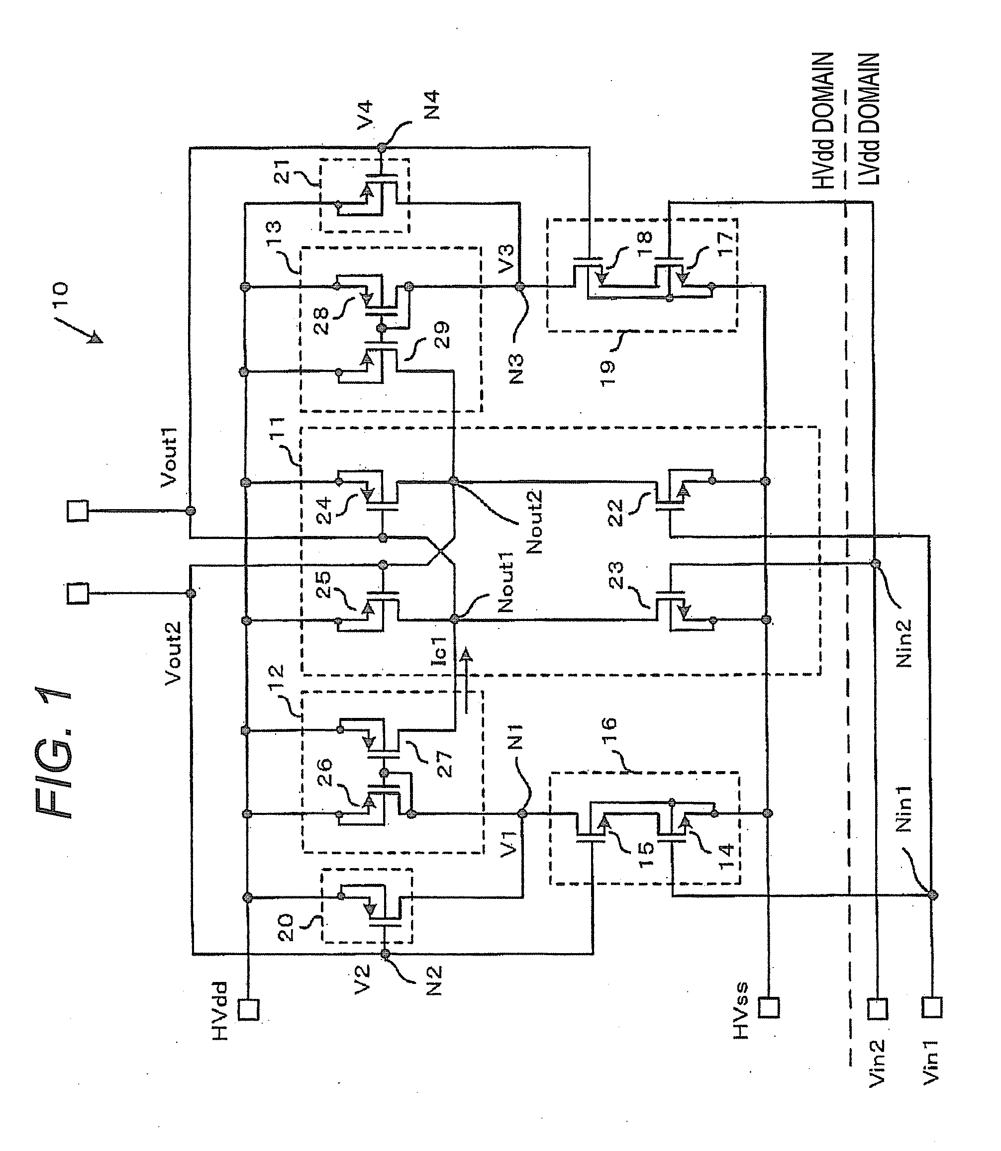
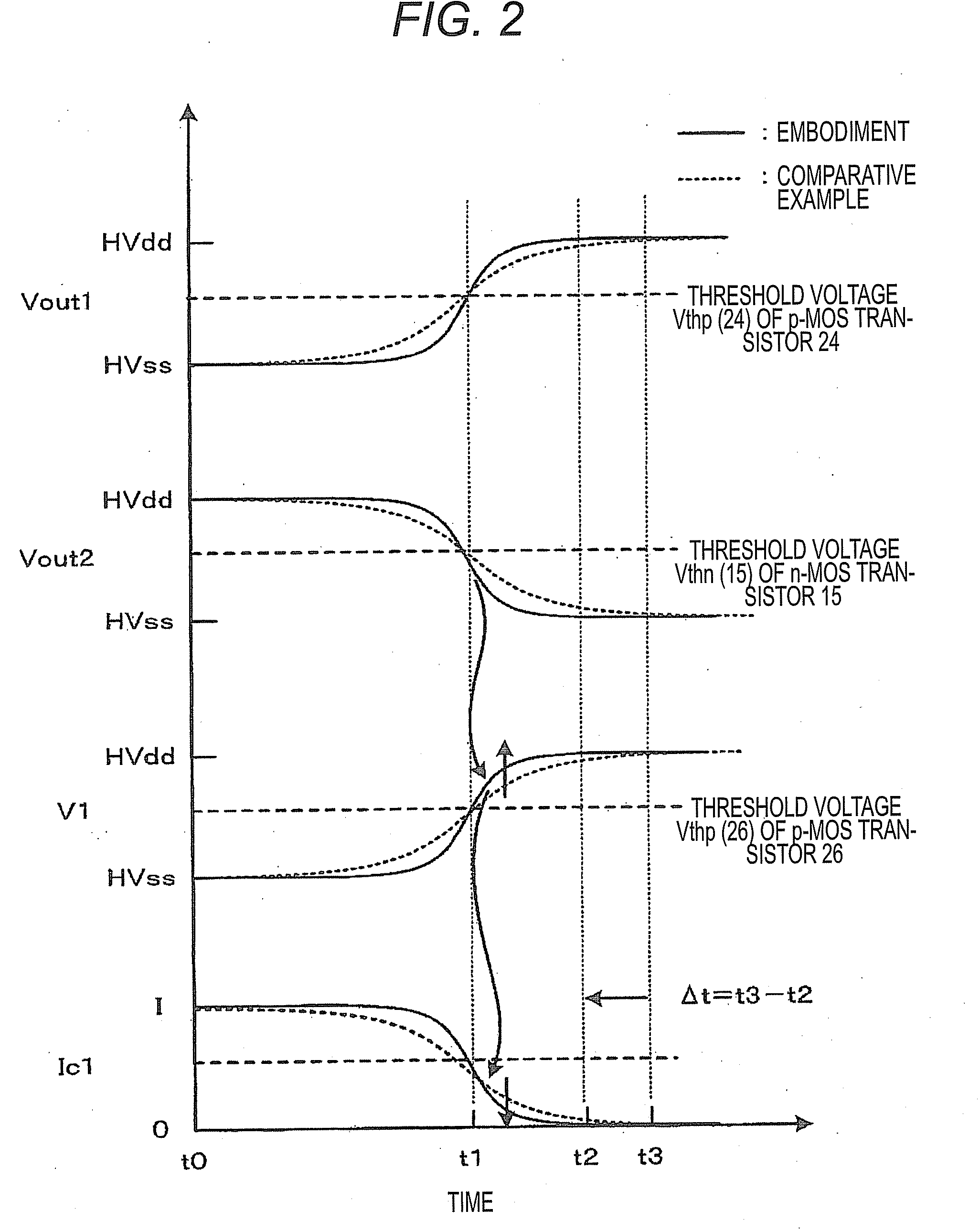
[0021]A semiconductor integrated device according to Embodiment 1 of the invention is described below by referring to FIGS. 1 to 3E. FIG. 1 is a circuit diagram of a semiconductor integrated device according to Embodiment 1. FIG. 2 is a timing chart illustrating an operation of the semiconductor integrated device 1 by being contrasted with that of a comparative example. FIGS. 3A to 3E are timing charts each illustrating an operation of the semiconductor integrated device by being contrasted with that of the comparative example.

[0022]As illustrated in FIG. 1, a semiconductor integrated device 10 according to the present embodiment includes a level-shifting circuit 11 configured to have a first input node Nin1 to which a first input signal Vin1 having a first amplitude is input, a second input node Nin2 to which a second input signal Vin2 obtained by inverting the first input signal Vin1 is input, a first output node Nout1 from which a first output signal Vout1 having a second amplitu...

embodiment 2

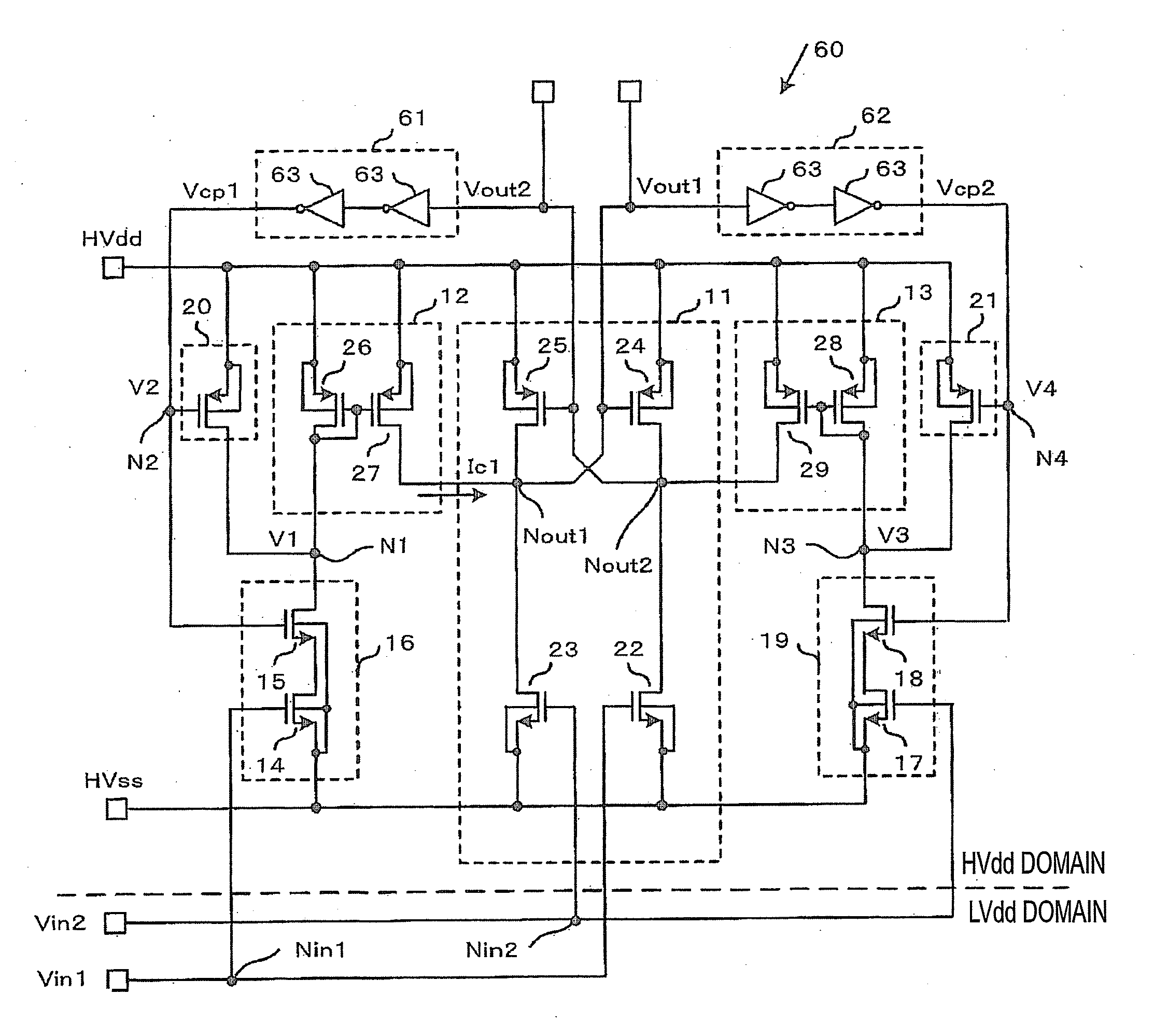
[0097]A semiconductor integrated device according to Embodiment 2 of the invention is described below with reference to FIGS. 5 to 7E. FIG. 5 is a circuit diagram of the semiconductor integrated device according to Embodiment 2. FIG. 6 is a timing chart illustrating an operation of the semiconductor integrated device by being contrasted with that of the comparative example. FIGS. 7A to 7E are timing charts each illustrating an operation of the semiconductor integrated device by being contrasted with that of the comparative example.

[0098]Components of the present embodiment, which are the same as those of the aforementioned Embodiment 1, are designated with the same reference numerals. Thus, the description of such components is omitted. In the following description of Embodiment 2, only components differing from those of Embodiment 1 are described below.

[0099]Embodiment 2 differs from Embodiment 1 in that inverters are connected between a second output node and a second node and bet...


PUM


Abstract

According to an aspect of the present invention, there is provided a semiconductor integrated device including: a level-shifting circuit including: a first and a second input nodes; and a first and a second output nodes; a first current mirror circuit connected with the first output node; a second current mirror circuit connected with the second output node; a first switch circuit series-connected with an input-side of first current mirror circuit; a second switch circuit series-connected with an input-side of the second current mirror circuit; a fifth switching element parallel-connected with the input-side of the first current mirror circuit; and a sixths switching element parallel-connected with the input-side of the second current mirror circuit.

Description

CROSS-REFERENCE TO RELATED APPLICATIONS[0001]This application claims priority from Japanese Patent Application No. 2008-058508 filed on Mar. 7, 2008, the entire contents of which are incorporated herein by reference.BACKGROUND OF THE INVENTION[0002]1. Field of the Invention[0003]An aspect of the present invention relates to a semiconductor integrated device.[0004]2. Description of the Related Art[0005]A conventional level-shifting circuit has first and second p-channel metal oxide semiconductor (PMOS) transistors, each of which is connected to the drain of an associated one of first and second n-channel metal oxide semiconductor (NMOS) transistors as a load and has a gate cross-connected to the drain of the other PMOS transistor. In the conventional level-shifting circuit, as a voltage difference between before and after the level-shifting increases, an output signal is not completely inverted even when an input signal is inverted, and an operation is unstable.[0006]Accordingly, alt...

Claims


Application Information

Patent Timeline
Patent Type & Authority Applications(United States)
IPC IPC(8): H03L5/00
CPCH03K3/35613
Inventor NAKAMURA, TETSUYAITO, HIDEAKI
Owner KK TOSHIBA
Why Eureka
Try Eureka