Patterning method in semiconductor manufacturing process

a semiconductor manufacturing and pattern transfer technology, applied in semiconductor/solid-state device manufacturing, basic electric elements, electric devices, etc., can solve the problem that the resolution of pattern transfer cannot be further improved, the optical lithography in semiconductor manufacturing processes has a dimension limitation, and the bottlenecks of manufacturing processes. achieve the effect of increasing the overlay accuracy

Active Publication Date: 2009-09-10
NAN YA TECH
View PDF2 Cites 12 Cited by
  • Summary
  • Abstract
  • Description
  • Claims
  • Application Information

AI Technical Summary

Benefits of technology

[0008]One particular aspect of the present invention is to provide a patterning method in a semiconductor manufacturing process. In addition to increase the overlay accuracy, the patterning method can produce a lot of two-dimension structures with a smaller dimension on a wafer substrate.

Problems solved by technology

However, there will be a lot of bottlenecks on the manufacturing processes due to limitations for reducing the dimension of the elements.
Currently, optical lithography in semiconductor manufacturing processes has a dimension limitation.
Due to the optical characteristic of the optics, the line width cannot be further reduced so that the resolution of the pattern transfer cannot be further improved.
Moreover, when the dimension of the electronic elements become smaller, the overlay accuracy of the photolithography process cannot be controlled well.
At the same time, the other lithography processes, such as E-beam lithography, EUV lithography etc., also has the development limitation on the throughput and the materials.

Method used


Image

  • Patterning method in semiconductor manufacturing process
  • Patterning method in semiconductor manufacturing process
  • Patterning method in semiconductor manufacturing process

Examples


Embodiment Construction

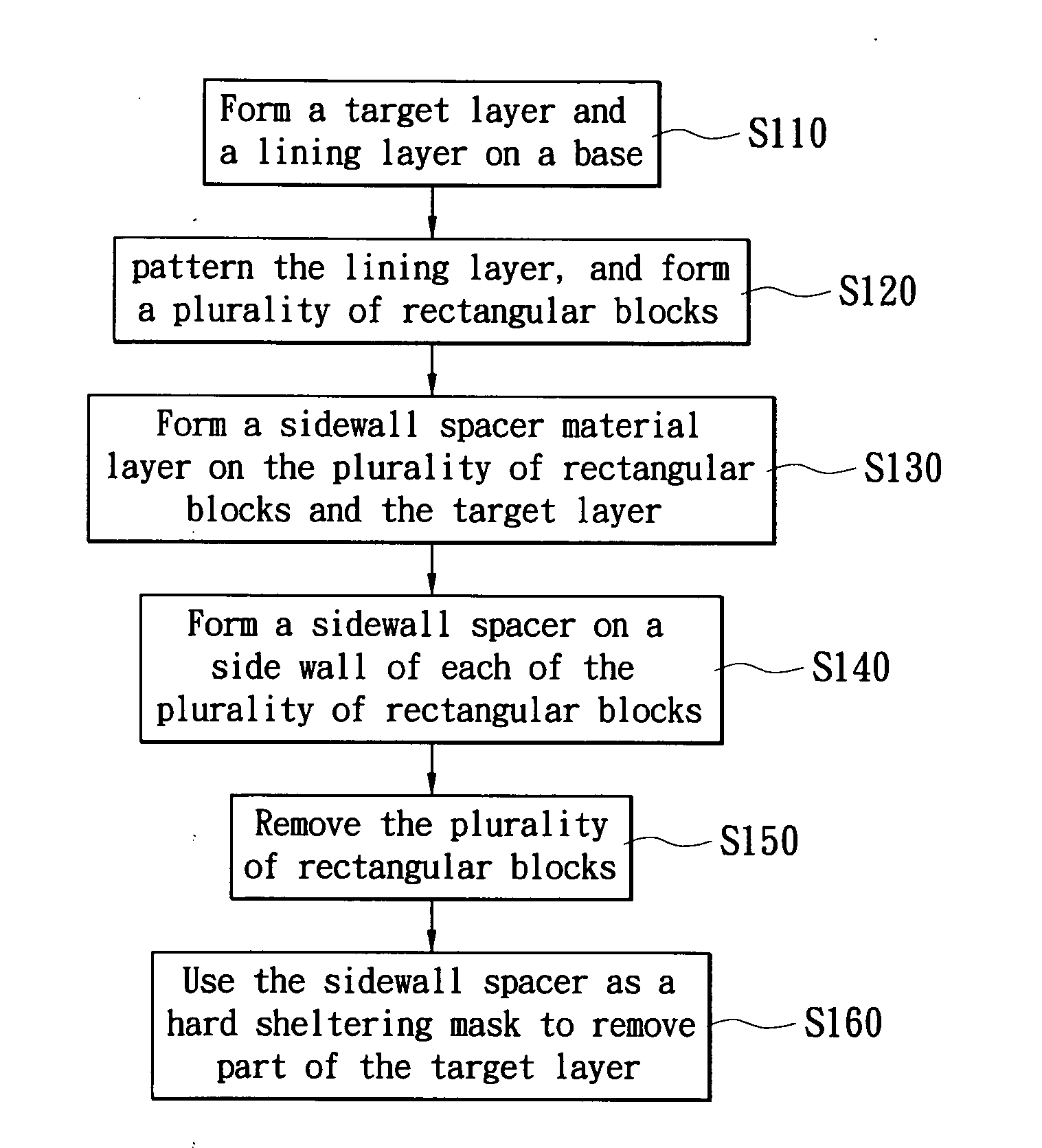
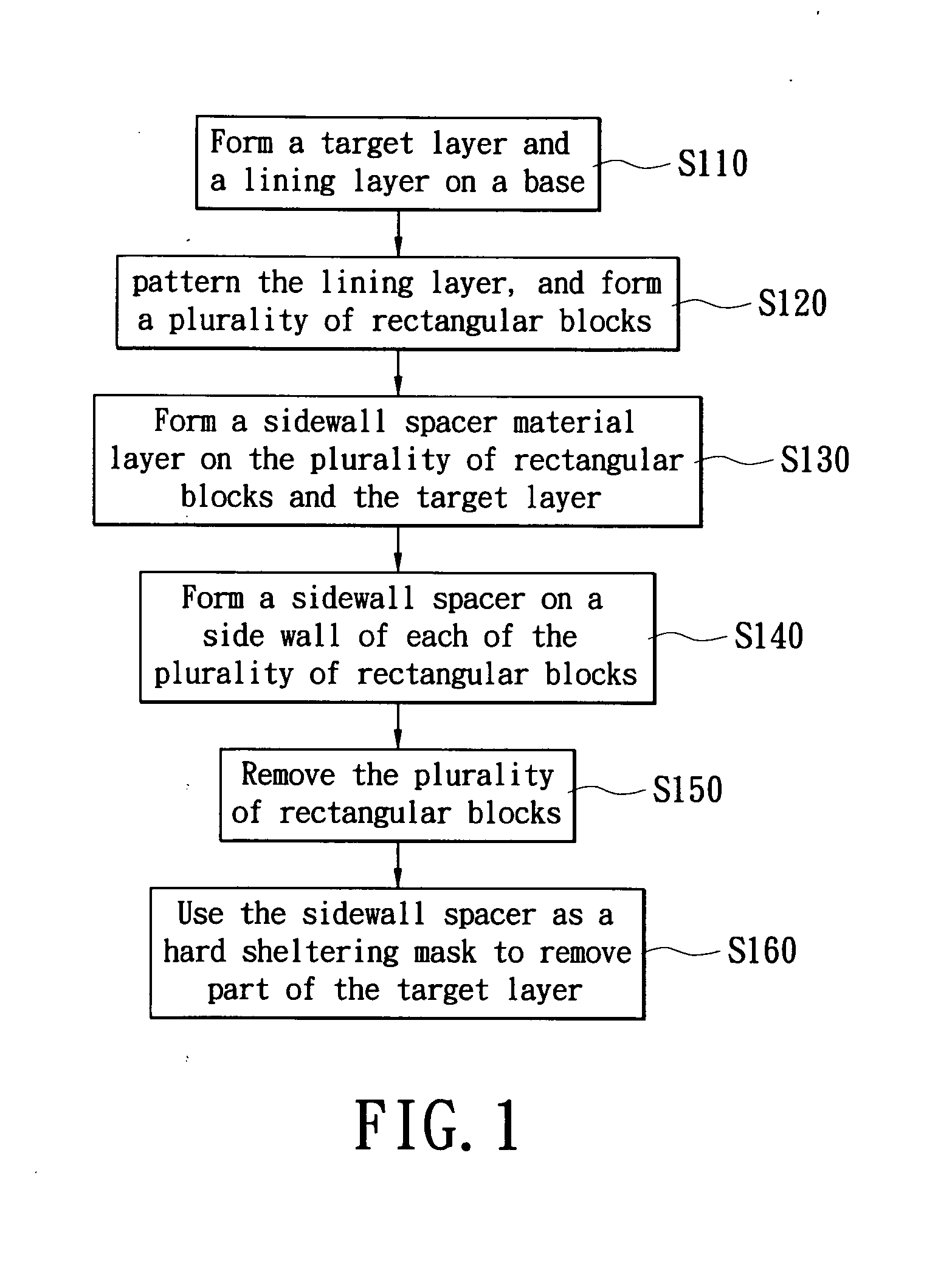
[0022]Reference is made to FIG. 1. The present invention discloses a patterning method including the following steps.

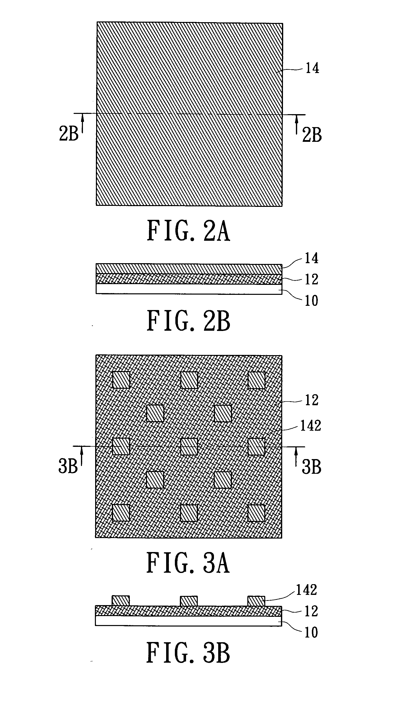
[0023]S110: First, a base is provided, and a target layer and a lining layer are sequentially formed on the surface of the base.

[0024]S120: A photolithography process is performed to pattern the lining layer and partially expose the surface of the target layer. The lining layer is formed with a plurality of rectangular blocks that are disposed by a checkerboard way on target layer. The checkerboard way means that the plurality of rectangular blocks is disposed on the target layer in a staggered way.

[0025]S130: A sidewall spacer material layer is conformally formed on the rectangular blocks and the target layer blocks.

[0026]S140: The sidewall spacer material layer is partially removed to form a sidewall spacer on the sidewall of each of the plurality of rectangular blocks, and exposes part of the surface of the target layer.

[0027]S150: The plurality of rectangular bloc...


PUM


Abstract

A patterning method in a semiconductor manufacturing process includes the following steps. A base is provided. A target layer and a lining layer are sequentially formed on the surface of the base. The lining layer is patterned to form a plurality of rectangular blocks. A sidewall spacer material layer is formed on the rectangular blocks and the target layer. Part of the sidewall spacer material layer is removed to form a sidewall spacer on the side wall of each of the plurality of rectangular blocks. The plurality of rectangular blocks is removed, and the sidewall spacer is used as a hard sheltering mask to etch and remove part of the target layer. The overlay accuracy is improved and the dimension of the electronic elements can be reduced so that a lot of two-dimension structures can be manufactured on the wafer substrate.

Description

BACKGROUND OF THE INVENTION[0001]1. Field of the Invention[0002]The present invention relates to a patterning method in a semiconductor manufacturing process. In particular, this invention relates to a patterning method by forming a patterned layer, forming a sidewall spacer on sidewalls of the patterned layer so as to provide two-dimensional blocks on a base in a semiconductor manufacturing process.[0003]2. Description of the Related Art[0004]As the semiconductor manufacturing process has been continuously developed, the dimension of the integrated circuit element is smaller than 100 nm. Commonly, the higher the quantity of the electronic elements on a unit area of the wafer substrate is, the higher the efficiency is (the quantity is higher, the operation speed is faster, and the required power is lower). When the quantity of the electronic elements on a unit area of the wafer substrate is further increased, electronic elements with smaller dimensions are required so that the manuf...

Claims


Application Information

Patent Timeline
Patent Type & Authority Applications(United States)
IPC IPC(8): H01L21/44
CPCH01L21/76816H01L21/0337
Inventor SHIU, WEI-CHENGWANG, YA-CHIH
Owner NAN YA TECH
Why Eureka
Try Eureka