Semiconductor storage device

a semiconductor and storage device technology, applied in the direction of semiconductor devices, resistors, electrical equipment, etc., can solve the problems of physical improvement limit, such as the breakdown voltage between devices, and the difficulty of overcoming such refinement challenges

Inactive Publication Date: 2009-09-17
KK TOSHIBA
View PDF4 Cites 220 Cited by
  • Summary
  • Abstract
  • Description
  • Claims
  • Application Information

AI Technical Summary

Problems solved by technology

Although the dimension for each device must be reduced (refined) to increase memory storage capacity, recent years are facing challenges in such refinement from the viewpoint of cost and technology.
However, in currently available ArF immersion lithography technology, for example, the resolution limit has been reached around the 40 nm design rule and so EUV exposure devices have to be introduced for further refinement.
However, the EUV exposure devices are expensive and infeasible in view of the costs.
In addition, if such refinement is accomplished, it is assumed that physical improvement limit, such as in breakdown voltage between devices, would be reached unless driving

Method used


Image

  • Semiconductor storage device
  • Semiconductor storage device
  • Semiconductor storage device

Examples


first embodiment

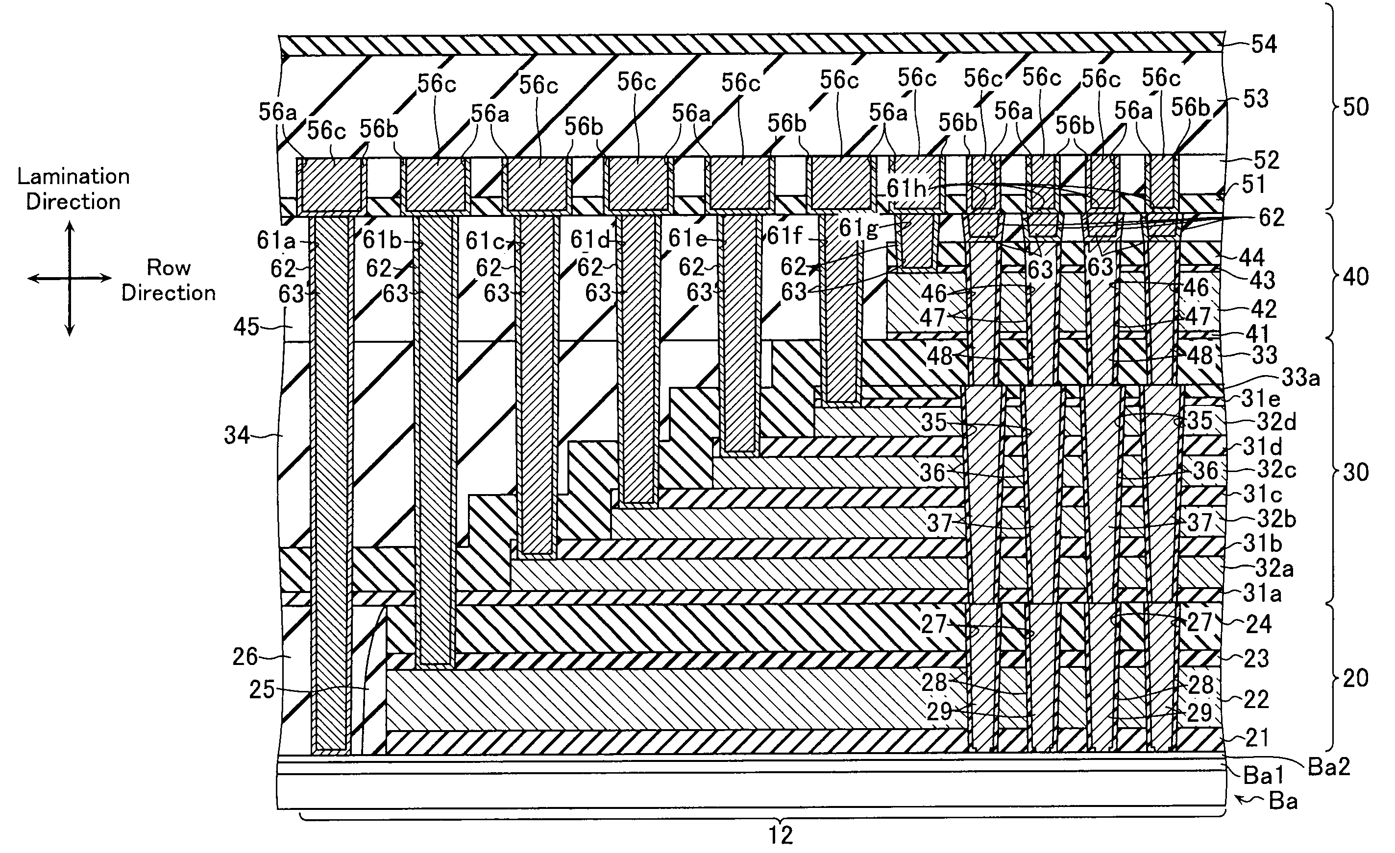
[0037](Configuration of Non-Volatile Semiconductor Storage Device 100 in First Embodiment)

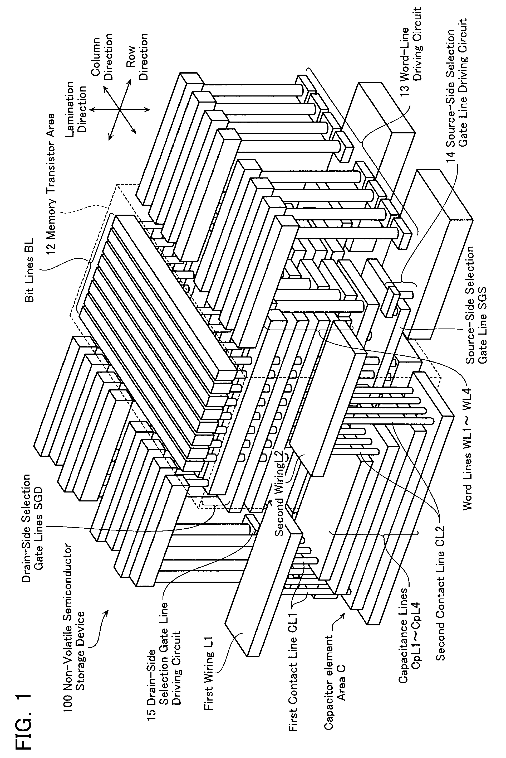
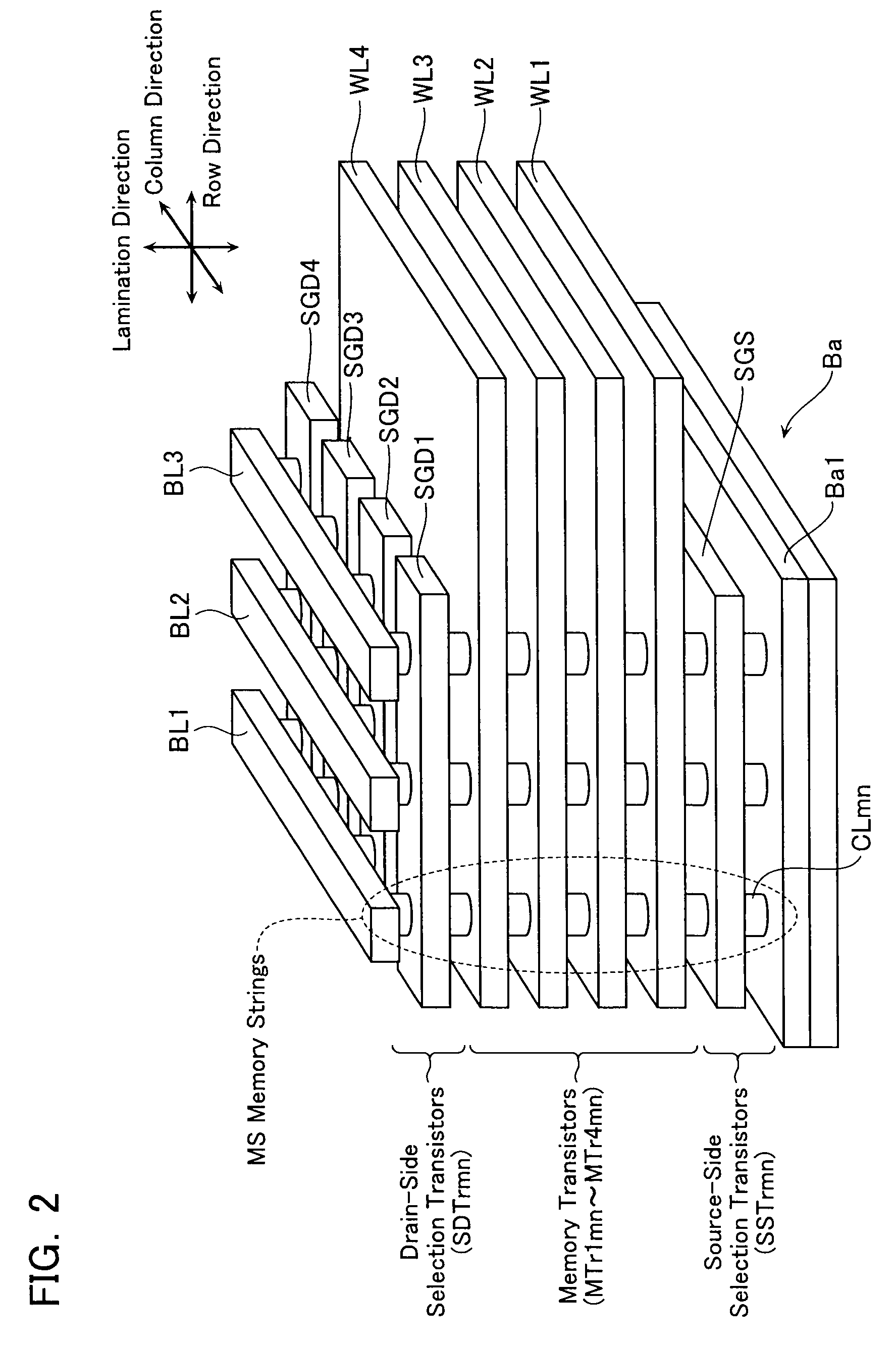
[0038]FIG. 1 schematically illustrates a non-volatile semiconductor storage device 100 according to a first embodiment of the present invention. As illustrated in FIG. 1, the non-volatile semiconductor storage device 100 according to the first embodiment mainly comprises: a memory transistor area 12; a word-line driving circuit 13; a source-side selection gate line (SGS) driving circuit 14; a drain-side selection gate line (SGD) driving circuit 15; a sense amplifier (not illustrated); and a capacitor element area C.

[0039]The memory transistor area 12 has memory transistors for storing data. The word-line driving circuit 13 controls voltage applied to word lines (first conductive layers) WL. The source-side selection gate line (SGS) driving circuit 14 controls voltage applied to the source-side selection gate line SGS. The drain-side selection gate line (SGD) driving circuit 15 controls voltage ...

second embodiment

[0112](Specific Configuration of Non-Volatile Semiconductor Storage Device in Second Embodiment)

[0113]Referring now to FIGS. 9 and 10, a configuration of a non-volatile semiconductor storage device according to a second embodiment of the present invention will be described below. FIG. 9 is a schematic cross-sectional view illustrating a part of a capacitor element area Ca in the non-volatile semiconductor storage device according to the second embodiment; and FIG. 10 is a top plan view thereof. Note that the same reference numerals represent the same components as the first embodiment and description thereof will be omitted in the second embodiment.

[0114]As illustrated in FIGS. 9 and 10, the non-volatile semiconductor storage device according to the second embodiment has a capacitor element area Ca different from the first embodiment. The second embodiment is different from the first embodiment in the configurations of first contact lines CL1′ and second contact lines CL2′ in the ca...

third embodiment

[0121](Configuration of Non-Volatile Semiconductor Storage Device in Third Embodiment)

[0122]Referring now to FIGS. 11 to 13A, a configuration of a non-volatile semiconductor storage device according to a third embodiment of the present invention will be described below. FIG. 11 is a schematic top plan view of the non-volatile semiconductor storage device according to the third embodiment. FIG. 12 is a cross-sectional view taken along the line I-I′ of FIG. 11; and FIG. 13A is a cross-sectional view taken along the line II-II′ of FIG. 11. Note that the same reference numerals represent the same components as the first and second embodiments and description thereof will be omitted in the third embodiment.

[0123]As illustrated in FIG. 11, the non-volatile semiconductor storage device according to the third embodiment comprises a memory transistor area 12a having a plurality of memory strings MSa, and a capacitor element area Cb having capacitor elements. In the memory transistor area 12a...


PUM


Abstract

A non-volatile semiconductor storage device has: a plurality of memory strings with a plurality of electrically rewritable memory cells connected in series; and a capacitor element area including capacitor elements. Each of the memory strings includes: a plurality of first conductive layers laminated on a substrate; and a plurality of first interlayer insulation layers formed between the plurality of first conductive layers. The capacitor element area includes: a plurality of second conductive layers laminated on a substrate and formed in the same layer as the first conductive layers; and a plurality of second interlayer insulation layers formed between the plurality of second conductive layers and formed in the same layer as the first interlayer insulation layers. A group of the adjacently-laminated second conductive layers is connected to a first potential, while another group thereof is connected to a second potential.

Description

CROSS REFERENCE TO RELATED APPLICATIONS[0001]This application is based on and claims the benefit of priority from prior Japanese Patent Application No. 2008-67544, filed on Mar. 17, 2008, and prior Japanese Patent Application No. 2008-68745, filed on Mar. 18, 2008, the entire contents of which are incorporated herein by reference.BACKGROUND OF THE INVENTION[0002]1. Field of the Invention[0003]The present invention relates to an electrically rewritable semiconductor storage device.[0004]2. Description of the Related Art[0005]Conventionally, LSIs are formed by integration of devices in a two-dimensional plane on the silicon substrate. Although the dimension for each device must be reduced (refined) to increase memory storage capacity, recent years are facing challenges in such refinement from the viewpoint of cost and technology. Such refinement requires further improvements in photolithography technology. However, in currently available ArF immersion lithography technology, for examp...

Claims


Application Information

Patent Timeline
IPC IPC(8): H01L29/792H01L27/105
CPCH01L27/0688H01L27/105H01L28/20H01L27/11582H01L27/11578H10B43/50H10B43/20H10B43/27H10B63/30
Inventor SAKAGUCHI, TAKESHINITSUTA, HIROYUKI
Owner KK TOSHIBA
Why Eureka
Try Eureka