Advanced quad flat no lead chip package having marking and corner lead features and manufacturing methods thereof

Active Publication Date: 2009-09-17
ADVANCED SEMICON ENG INC
View PDF99 Cites 100 Cited by
  • Summary
  • Abstract
  • Description
  • Claims
  • Application Information

AI Technical Summary

Problems solved by technology

Semiconductor chips have become progressively more complex, driven in large part by the need for increasing processing power in a smaller chip size.
However, manufacturing processes for such leadframes may not be scalable beyond two rows of leads.
For example, it may be difficult to determine how to properly orient the package during surface mounting to the PCB.
For example, stress due to differential thermal expansion between the leads and the package body may be concentrated at the corners of the package, which can lead to cracking of solder connections to the PCB near the corners of the package, and thus to a decrease in the reliability of surface mounting.
Current packaging solutions can meet some of these objectives but may not be able to meet most, or all, of these objectives.

Method used


Image

  • Advanced quad flat no lead chip package having marking and corner lead features and manufacturing methods thereof
  • Advanced quad flat no lead chip package having marking and corner lead features and manufacturing methods thereof
  • Advanced quad flat no lead chip package having marking and corner lead features and manufacturing methods thereof

Examples


Embodiment Construction

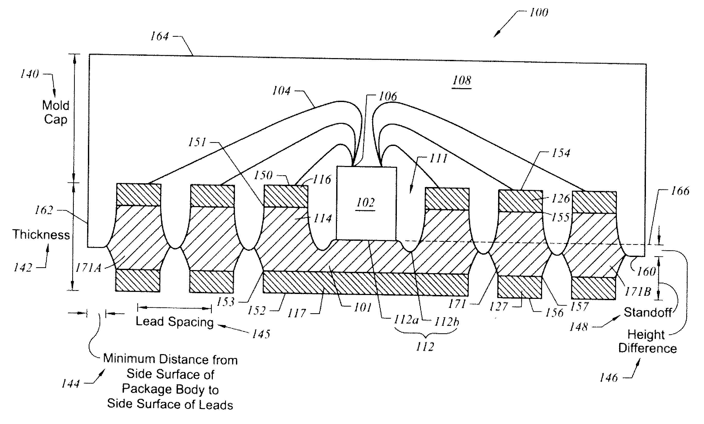
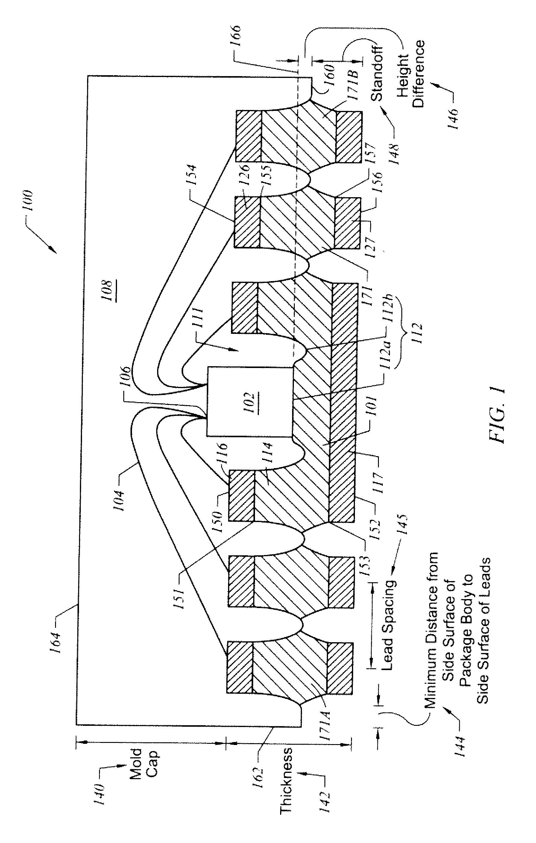
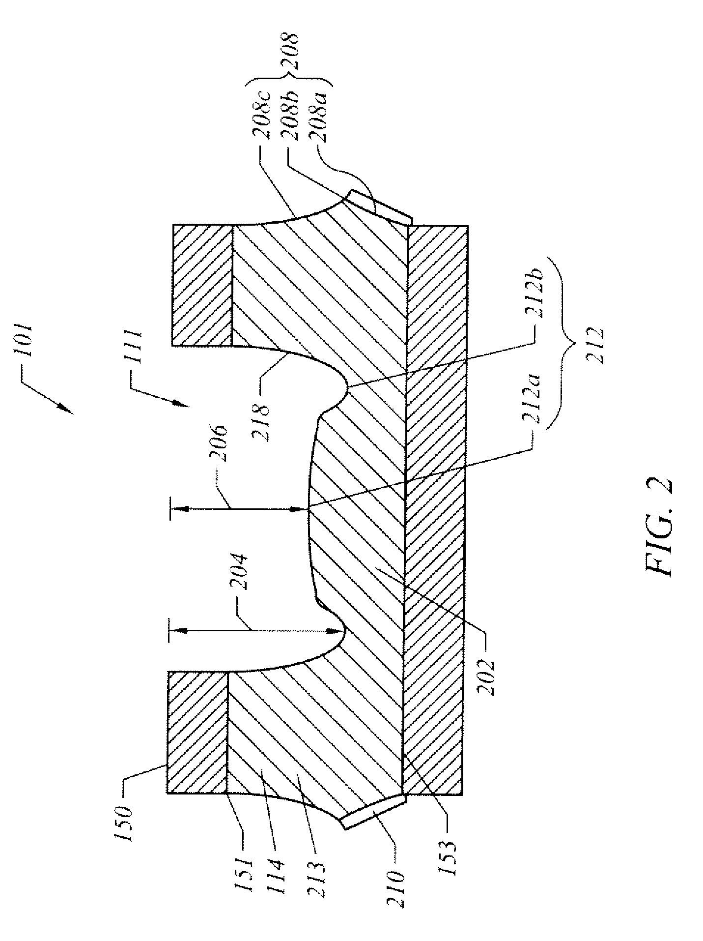
[0022]FIG. 1 illustrates a cross-sectional view of a semiconductor package 100, in accordance with one embodiment of the present invention. The package 100 includes a die pad 101 with a peripheral edge region 114 that defines a cavity 111 with a cavity bottom 112. The peripheral edge region 114 may completely surround the cavity 111, but also can partially surround the cavity 111 for certain implementations. The cavity bottom 112 includes a central portion 112a. The cavity bottom 112 may also include a recess 112b around the central portion 112a. The central portion 112a may be approximately centrally located within the cavity bottom 112, but need not be it; for example, the recess 112b is of non-uniform width. The recess 112b may completely surround the central portion 112a, but also can partially surround the central portion 112a for certain implementations. A chip 102 is attached to the cavity bottom 112 by an adhesive layer (not shown). The adhesive layer may be a conductive or ...


PUM


Abstract

A semiconductor package and related methods are described. In one embodiment, the package includes a die pad, a first plurality of leads disposed in a lead placement area around the die pad, a second plurality of leads disposed in corner regions of the lead placement area, a semiconductor chip on the die pad and coupled to each lead, and a package body. Each lead includes an upper sloped portion and a lower sloped portion. An average of surface areas of lower surfaces of each of the second plurality of leads is at least twice as large as an average of surface areas of lower surfaces of each of the first plurality of leads. The package body substantially covers the upper sloped portions of the leads. The lower sloped portions of the leads at least partially extend outwardly from a lower surface of the package body.

Description

CROSS-REFERENCE TO RELATED APPLICATION[0001]The present application claims the benefit of the following commonly owned U.S. provisional patent application, which is incorporated herein by reference in its entirety U.S. Provisional Patent Application No. 61 / 036,470, Attorney Docket No. ASEG-001 / 00US entitled “Chip Package Structure and Manufacturing Methods Thereof,” filed on Mar. 14, 2008.FIELD OF THE INVENTION[0002]The present invention relates generally to semiconductor chip packages. More particularly, this invention relates to an advanced Quad Flat No Lead (aQFN) chip package having marking and corner lead features and manufacturing methods thereof.BACKGROUND OF THE INVENTION[0003]Semiconductor chips have become progressively more complex, driven in large part by the need for increasing processing power in a smaller chip size. In response. packaging technologies have evolved, for example, to enable an increased lead density, which can reduce the footprint area of a package mount...

Claims


Application Information

Patent Timeline
IPC IPC(8): H01L23/495H01L21/60
CPCH01L21/4832H01L23/3107H01L2924/07802H01L2224/73265H01L2224/32145H01L2924/12041H01L2224/32245H01L2924/01087H01L24/48H01L2924/30105H01L2924/19041H01L2924/01082H01L2924/01079H01L2924/01078H01L2924/01075H01L2924/01046H01L2924/01033H01L2924/01029H01L2924/01013H01L2924/01002H01L2224/97H01L2224/92247H01L2224/48247H01L2224/48091H01L2224/32257H01L23/49548H01L23/49582H01L24/97H01L2224/85H01L2924/00014H01L2924/00012H01L2924/00H01L24/73H01L2924/181H01L2224/49433H01L2224/45099H01L2224/45015H01L2924/207
Inventor CHANG CHIEN, PAO-HUEIHU, PING-CHENGCHEN, CHIEN-WEN
Owner ADVANCED SEMICON ENG INC
Why Eureka
Try Eureka