Semiconductor device and method for manufacturing the same

a semiconductor and semiconductor technology, applied in the direction of semiconductor devices, semiconductor/solid-state device details, electrical devices, etc., to achieve the effect of reducing the oxidized part more effectively and reducing the oxidized portion

Inactive Publication Date: 2009-09-17
TOKYO ELECTRON LTD
View PDF5 Cites 14 Cited by
  • Summary
  • Abstract
  • Description
  • Claims
  • Application Information

AI Technical Summary

Benefits of technology

[0019]The blowing step may include a step of exciting the organosilane gas and the hydrogen gas by applying a microwave thereto. By applying this means to the method for manufacturing a semiconductor, it is possible to reduce the oxidized part more effectively compared with another case in which the organosilane gas and the hydrogen gas are just blown to the oxidized part of the interconnection material.
[0020]The blowing step may be to blow the organosilane gas and the hydrogen gas after raising temperature of the substrate within a range from 150 to 350 degrees Celsius. By applying this means to the method for manufacturing a semiconductor, it is possible to reduce the oxidized portion more effectively compared with another case in which the organosilane gas and the hydrogen gas are just blown to the oxidized part of the interconnection material.

Problems solved by technology

In particular, in a case a fluorocarbon film is used as the interlayer insulating film, the method described above is more effective because the fluorocarbon film has a poor resistance to the damage caused by the reduction treatment.

Method used


Image

  • Semiconductor device and method for manufacturing the same
  • Semiconductor device and method for manufacturing the same
  • Semiconductor device and method for manufacturing the same

Examples


Embodiment Construction

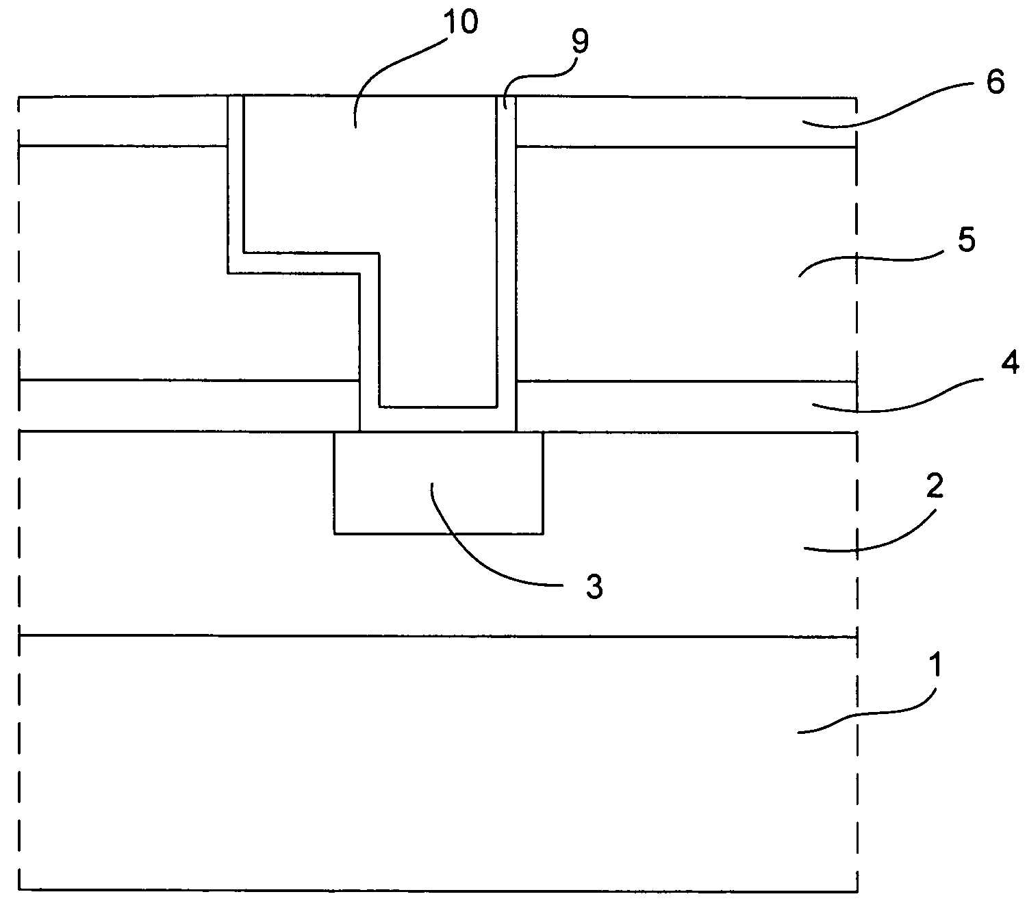
[0042]Firstly, a method for manufacturing a semiconductor of the present invention will be explained. As the method, for example, conventional Dual Damascene and Single Damascene and the like can be used. Concretely, the method of the present invention includes the following steps.

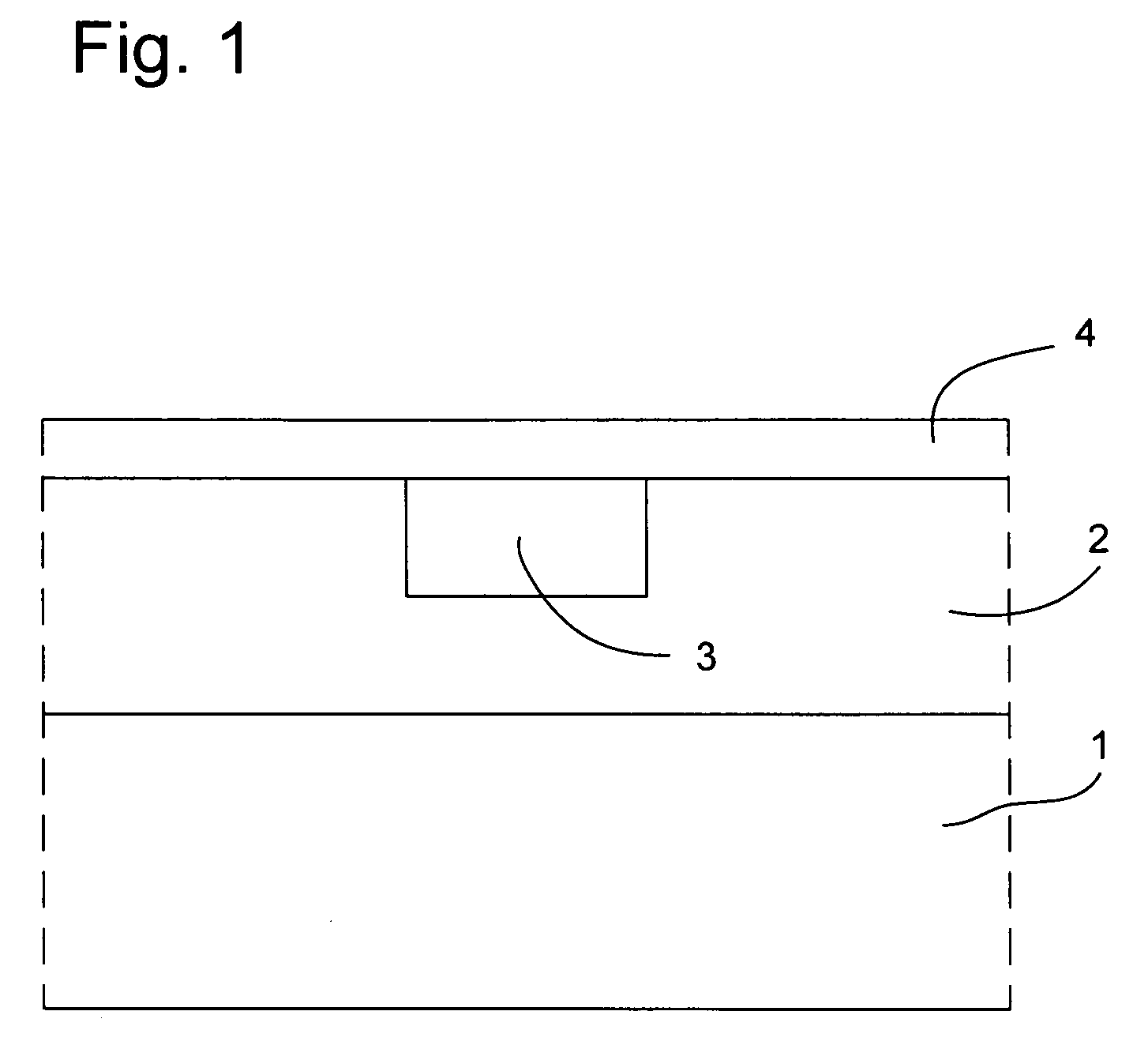
[0043]1) forming a first interlayer insulating film on a substrate, wherein a conductor is embedded in the first interlayer insulating film;

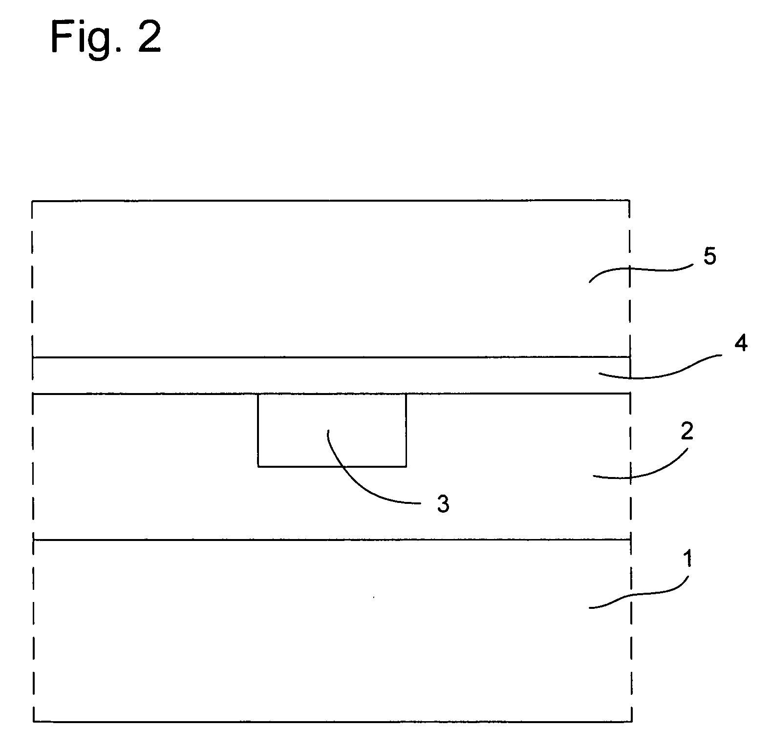
[0044]2) forming an etch stop layer on the first interlayer insulating film and the conductor;

[0045]3) forming a second interlayer insulating film and a cap layer on the etch stop layer;

[0046]4) forming a via hole and an interconnection groove which pass through the second interlayer insulating film and the cap layer;

[0047]5) removing the etch stop layer by etching;

[0048]6) blowing an organosilane gas and a hydrogen gas to the surface of the conductor exposed externally and side walls of the via hole and the interconnection groove;

[0049]7) forming a barrier layer on th...


PUM


Abstract

The present invention is a method for manufacturing a semiconductor device having a conductor and an insulating film on a substrate, the method including the steps of forming the conductor on the substrate, forming the insulating film on the conductor, removing the insulating film on the conductor, and blowing an organosilane gas and a hydrogen gas to reduce an oxidized region on the conductor, wherein the oxidized region on the conductor is formed when the insulating film is removed.

Description

[0001]This application claims priority from U.S. provisional application Ser. No. 61 / 069244, filed Mar. 12, 2008, entitled “Film Forming Method”, which is incorporated herein by reference in its entirety.TECHNICAL FIELD[0002]The present invention relates to a semiconductor device and a method for manufacturing a semiconductor device. In particular, the present invention relates to a method for reducing an interconnection material (conductor) in the method for manufacturing the semiconductor device.BACKGROUND OF THE INVENTION[0003]As described in Japanese Unexamined Patent Application Publication No. 2004-71956, an exposed copper (Cu) interconnection, which was exposed by an etching step, an ashing step, and a subsequent washing step, can easily be oxidized. Ordinary, as a pretreatment of a step for foaming upper interconnection layers, a reduction treatment is conducted in a state where a substrate is heated using a reducing gas including NH3 and the like or an inactive gas in order...

Claims


Application Information

Patent Timeline
Patent Type & Authority Applications(United States)
IPC IPC(8): H01L21/44H01L29/40
CPCH01L21/02063H01L21/3105H01L21/76834H01L21/76807H01L21/76814H01L21/67207H01L21/3205H01L21/768
Inventor MATSUOKA, TAKAAKI
Owner TOKYO ELECTRON LTD
Why Eureka
Try Eureka