

Display Device and Driving Method Thereof
a technology of display device and driving method, which is applied in the direction of instruments, computing, electric digital data processing, etc., can solve the problems of image quality degradation, and achieve the effect of reducing the number of elements and wires that make up the screen and improving image quality
- Summary
- Abstract
- Description
- Claims
- Application Information
AI Technical Summary
Benefits of technology
Problems solved by technology
Method used
Image

Examples
embodiment 1
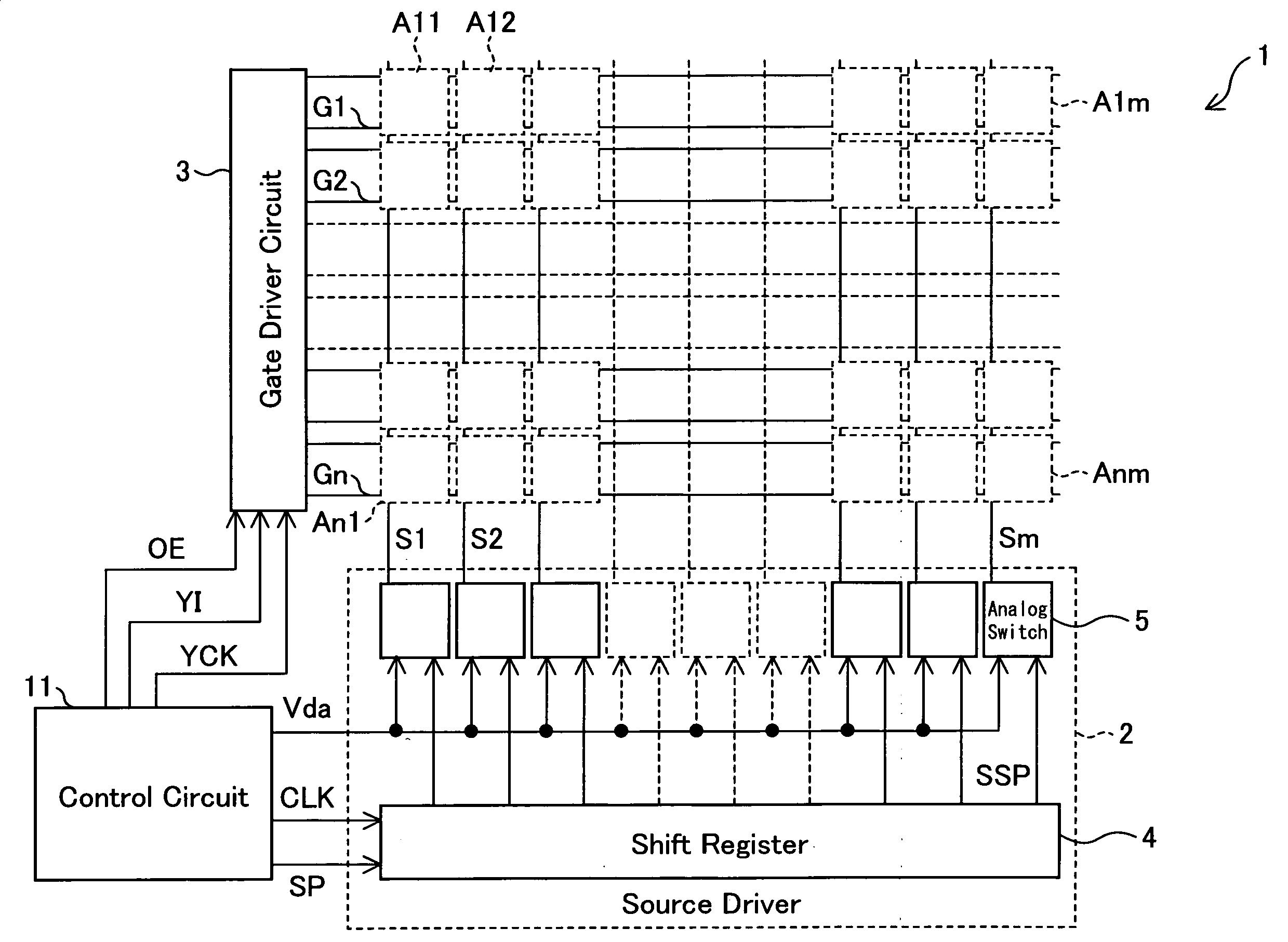
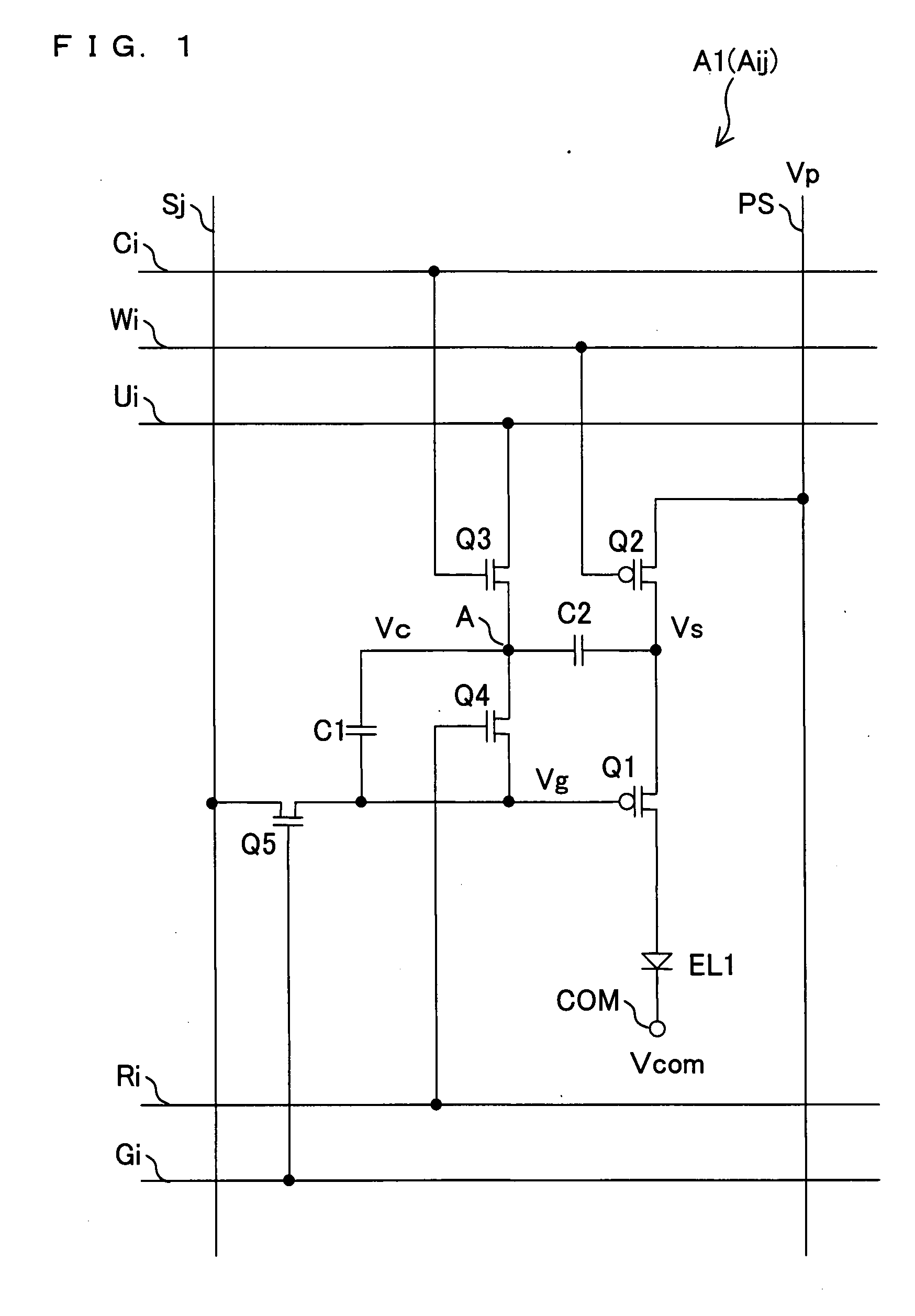
[0089]FIG. 1 is a circuit diagram illustrating the structure of a pixel circuit A1 in a display device 1 of the present embodiment. FIG. 2 depicts in a block diagram the overall circuit structure of the display device 1 of the present embodiment.
[0090]The display device 1 includes pixel circuits Aij (i=1 to n; j=1 to m), a source driver circuit 2, a gate driver circuit 3, and a control circuit 11 as shown in FIG. 2. The display device 1 further includes source lines Sj (signal lines), positioned parallel to one another, and gate lines Gi, positioned parallel to one another and orthogonal to the source lines Sj. The pixel circuit (pixels) Aij are each located where a source line Sj intersects a gate line Gi, forming a matrix as a whole. The source lines Sj are connected to the source driver circuit 2 to supply signals to the OLEDs EL1 (FIG. 1; will be detailed later). The gate lines Gi are connected to the gate driver circuit 3.
[0091]The driver circuits 2, 3 are preferably entirely o...
embodiment 2
[0157]The pixel circuit structure in FIG. 1 described in embodiment 1 contains not only n-type TFTs, but also p-type TFTs. The present invention is applicable, however, to structures that involve only n-type TFTs, such as amorphous silicon TFTs. The present embodiment will focus on those pixel circuit structures.
[0158]The same display device 1 as the one shown in FIG. 2 is used in the present embodiment; its description will not be repeated. In addition, the same elements in the pixel circuit Aij as those in the pixel circuit A1 (FIG. 1) in embodiment 1 are identified by the same reference symbols and their description is hot repeated here.
[0159]FIG. 8 is a circuit diagram illustrating the structure of a pixel circuit A2 (Aij) in the display device 1 of the present embodiment.
[0160]Referring to FIG. 8, the pixel circuit A2 has transistors (n-type TFTs) Q21 to Q25, capacitors C11, C12, and an OLED (electro-optical element) EL1.
[0161]In the pixel circuit A2, the transistor (driver tra...
embodiment 3
[0184]The pixel circuit structures in embodiments 1, 2 (FIGS. 1, 8) needs five horizontal wires. Among them, the potential line Ui may be shared by the pixel circuits A (i−1)j, A(i+1)j connected respectively to the two gate lines Gi−1, Gi+1 that are adjacent to the gate line Gi. The gate line Gi and the control line Ri, Wi, Ci cannot be shared by the pixel circuits A (i−1)j, A(i+1)j.
[0185]Accordingly, the present embodiment will describe a pixel circuit structure from which the control line Ci is omitted. FIG. 10 is a circuit diagram illustrating the structure of such a pixel circuit A3 (Aij).
[0186]Referring to FIG. 10, the pixel circuit A3 of the present embodiment replaces the n-type transistor Q4 in the pixel circuit A1 of embodiment 1 (FIG. 1) with a p-type transistor Q6, omits the control line Ci connected to the gate of the transistor Q3, and has the control line Ri connected to the gate of the transistor Q3. Otherwise, pixel circuit A3 is the same as the pixel circuit A1 in F...
PUM
 Abstract
Description
Claims
Application Information