Mono-energetic neutral beam activated chemical processing system and method of using

Active Publication Date: 2009-09-24
TOKYO ELECTRON LTD
View PDF14 Cites 143 Cited by
  • Summary
  • Abstract
  • Description
  • Claims
  • Application Information

AI Technical Summary

Benefits of technology

[0002]The invention relates to a method and system for treating a substrate and, more particularly, to a method and system for performing neutral beam activated chemical processing of a substrate.

Problems solved by technology

However, although RIE has been in use for decades, its maturity is accompanied by several issues including: (a) broad ion energy distribution (IED), (b) various charging-induced side effects; and (c) feature-shape loading effects (i.e., micro loading).
However, an adverse consequence of the lack of micro loading is the achievement of an etch efficiency of unity, i.e., the maximum etching yield is unity, or one incident neutral nominally prompts only one etching reaction.

Method used


Image

  • Mono-energetic neutral beam activated chemical processing system and method of using
  • Mono-energetic neutral beam activated chemical processing system and method of using
  • Mono-energetic neutral beam activated chemical processing system and method of using

Examples


Embodiment Construction

[0020]In the following description, to facilitate a thorough understanding of the invention and for purposes of explanation and not limitation, specific details are set forth, such as a particular geometry of the plasma processing system and various descriptions of the system components. However, it should be understood that the invention may be practiced with other embodiments that depart from these specific details.

[0021]Nonetheless, it should be appreciated that, contained within the description are features which, notwithstanding the inventive nature of the general concepts being explained, are also of an inventive nature.

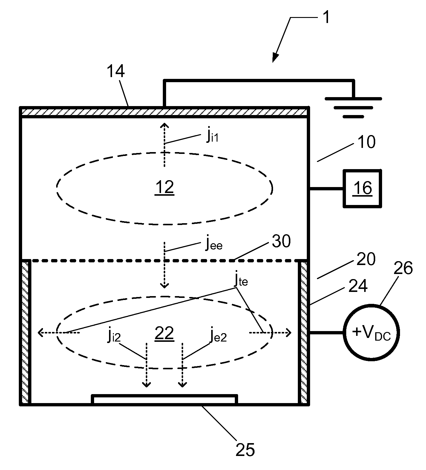
[0022]According to one embodiment, a method and system for performing neutral beam activated chemical processing of a substrate is provided, inter alia, to alleviate some or all of the above identified issues. Neutral beam activated chemical processing includes kinetic energy activation (i.e., thermal neutral species) and, hence, it achieves high reactive or et...


PUM

PropertyMeasurementUnit
DC voltageaaaaaaaaaa
frequencyaaaaaaaaaa
electron densityaaaaaaaaaa

Abstract

A chemical processing system and a method of using the chemical processing system to treat a substrate with a mono-energetic space-charge neutralized neutral beam-activated chemical process is described. The chemical processing system comprises a first plasma chamber for forming a first plasma at a first plasma potential, and a second plasma chamber for forming a second plasma at a second plasma potential greater than the first plasma potential, wherein the second plasma is formed using electron flux from the first plasma. Further, the chemical processing system comprises a substrate holder configured to position a substrate in the second plasma chamber.

Description

BACKGROUND OF THE INVENTION[0001]1. Field of the Invention[0002]The invention relates to a method and system for treating a substrate and, more particularly, to a method and system for performing neutral beam activated chemical processing of a substrate.[0003]2. Description of Related Art[0004]During semiconductor processing, plasma is often utilized to assist etch processes by facilitating the anisotropic removal of material along fine lines or within vias (or contacts) patterned on a semiconductor substrate. Examples of such plasma assisted etching include reactive ion etching (RIE), which is in essence an ion activated chemical etching process.[0005]However, although RIE has been in use for decades, its maturity is accompanied by several issues including: (a) broad ion energy distribution (IED), (b) various charging-induced side effects; and (c) feature-shape loading effects (i.e., micro loading). One approach to alleviate these problems is to utilize neutral beam processing.[000...

Claims


Application Information

Patent Timeline
Patent Type & Authority Applications(United States)
IPC IPC(8): C23F1/00C23F1/08
CPCH01J37/32091H01J37/321H01J37/3255H01J37/32357H01J37/32192H01J37/3244C23C16/44H01J37/32027H01J37/32422H01J2237/3341H01L21/3065
Inventor CHEN, LEE
Owner TOKYO ELECTRON LTD
Why Eureka
Try Eureka