Circuitized substrate and method of making same

a circuitized substrate and substrate technology, applied in the direction of printed circuits, electrical devices, printed circuit aspects, etc., can solve the problems of signal deterioration and various detrimental effects of high-speed connections, and achieve the effect of low cos

Inactive Publication Date: 2009-10-01
I3 ELECTRONICS
View PDF17 Cites 77 Cited by
  • Summary
  • Abstract
  • Description
  • Claims
  • Application Information

AI Technical Summary

Benefits of technology

[0032]It is still another object of the invention to provide such a method which may be accomplished in a relatively facile manner and at relatively low cost in comparison to some known substrate manufacturing processes.
[0033]According to one aspect of the invention, there is provided a method of making a circuitized substrate comprising providing a first dielectric layer having a first thickness, forming a conductive circuit on this first dielectric layer, bonding a second dielectric layer having a second thickness to the first dielectric layer such that the first and second dielectric layers will have a combined, third thickness, forming a first plurality of holes within the first and second dielectric layers, this first plurality of holes extending through both first and second dielectric layers, bonding third and fourth dielectric layers to the first and second dielectric layers, respectively, forming a second plurality of holes within each of these third and fourth dielectric layers, each of this second plurality of holes being in alignment with a respective one of the first plurality of holes to thereby form a plurality of continuous holes through the first, second, third and fourth dielectric layers, and positioning a quantity of conductive paste within each of these continuous holes to thereby form a plurality of continuous thru-holes each having a length such that the conductive paste within each of these thru-holes will possess a relatively low resistivity.

Problems solved by technology

Such high speed connections are subjected to various detrimental effects, e.g., signal deterioration (also referred to as signal attenuation), caused by the inherent characteristics of such known substrate circuitry wiring.

Method used


Image

  • Circuitized substrate and method of making same
  • Circuitized substrate and method of making same
  • Circuitized substrate and method of making same

Examples


Embodiment Construction

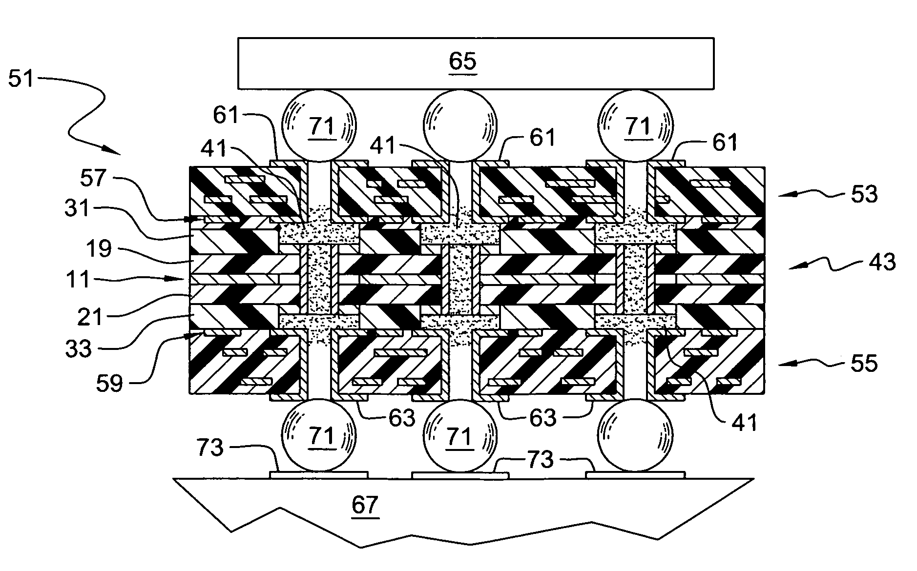
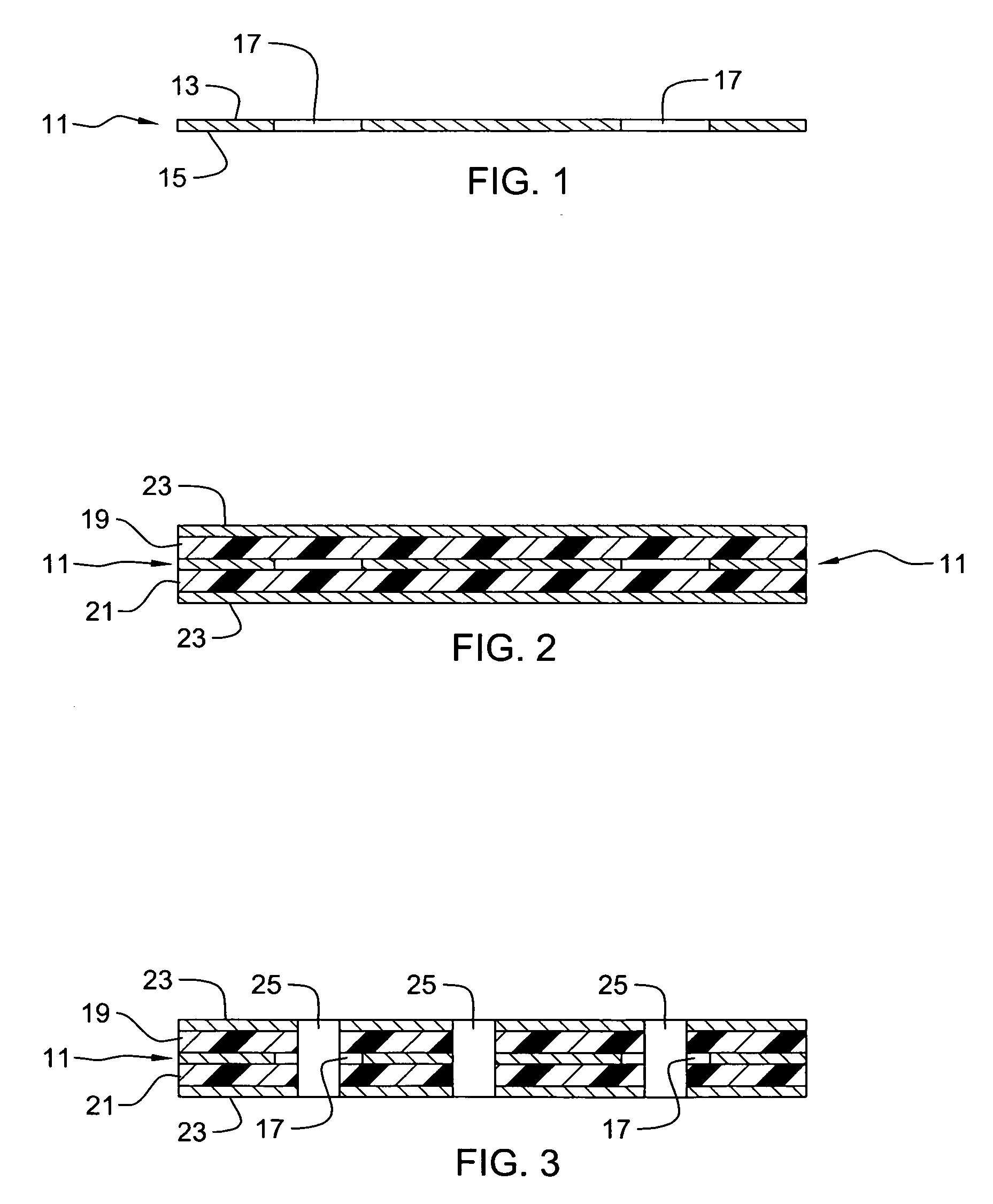
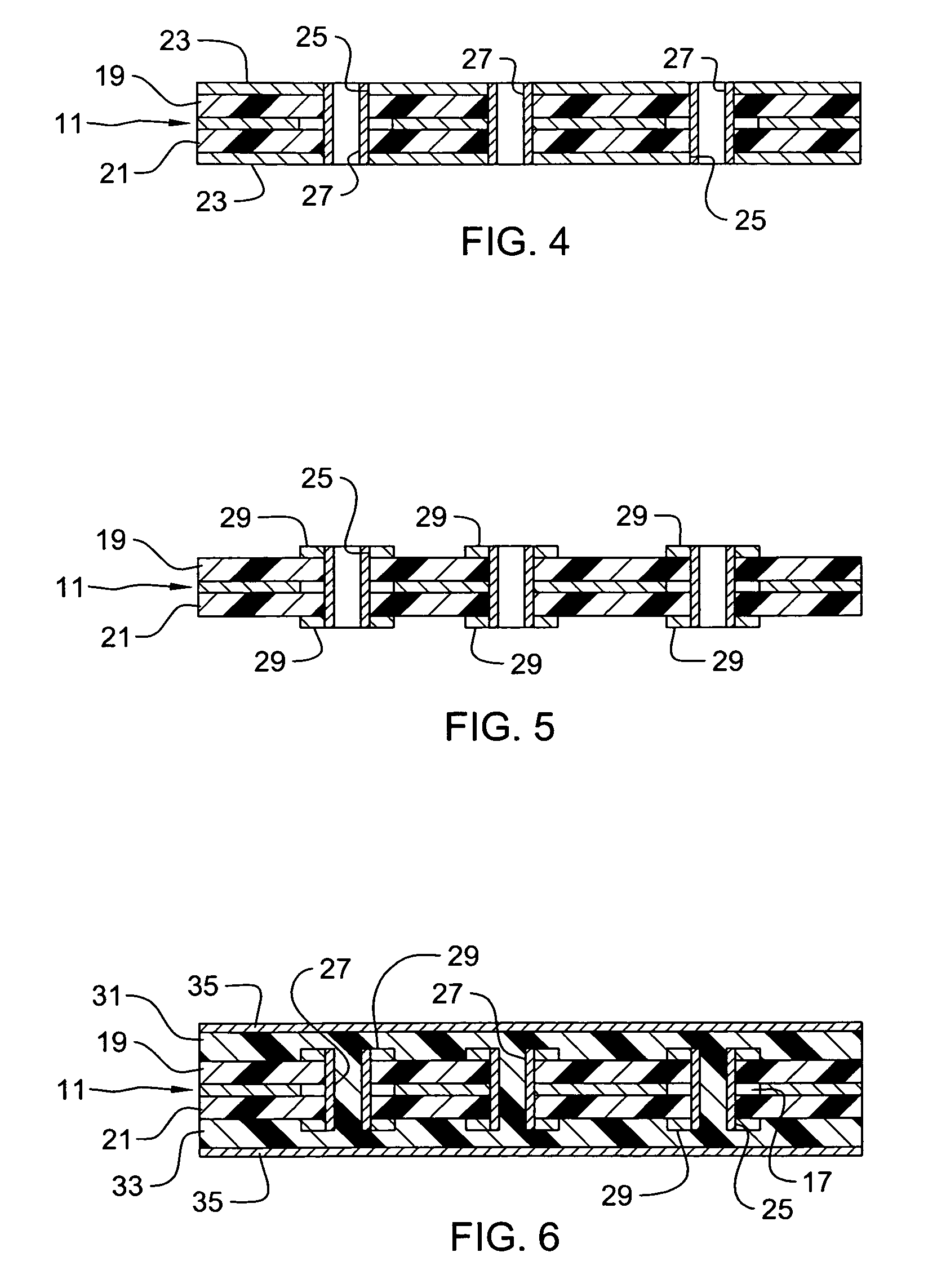
[0037]For a better understanding of the present invention, together with other and further objects, advantages and capabilities thereof, reference is made to the following disclosure and appended claims in connection with the above-described drawings. It is understood that like numerals will be used to indicate like elements from drawing figure to drawing figure.

[0038]The following terms will be used herein and are understood to have the meanings associated therewith.

[0039]By the term “circuitized substrate” is meant to include substrates including at least one and preferably more dielectric layers and at least one and preferably more conductive layers therein / thereon. Examples of dielectric materials suitable for use herein include fiberglass-reinforced or non-reinforced epoxy resins, polytetrafluoroethylene (Teflon), polyimides, polyamides, cyanate resins, photoimageable materials, ceramic and other like materials, or combinations thereof. Examples of materials for the conductive ...


PUM

PropertyMeasurementUnit
impedanceaaaaaaaaaa
thickaaaaaaaaaa
thicknessaaaaaaaaaa

Abstract

A circuitized substrate and method of making same in which a first plurality of holes are formed within two bonded dielectric layers and then made conductive, e.g., plated. The substrate also includes third and fourth dielectric layers bonded to the first and second with a plurality of continuous electrically conductive thru holes extending through all four dielectric layers. Conductive paste is positioned within the thru holes for providing electrical connections between desired conductive layers of the substrate and outer layers as well. A circuitized substrate assembly and method of making same are also provided.

Description

TECHNICAL FIELD [0001]The present invention relates to circuitized substrates, and more particularly to multilayered circuitized structures such as printed circuit boards (PCBs) and chip carriers. The present invention also relates to methods for fabricating such structures.BACKGROUND OF THE INVENTION [0002]A common method of forming a multi-layered circuitized substrate involves forming sub-composites each including an individual layer of dielectric material and a layer of electrically conducting material thereon, and then forming electrical circuit patterns in the electrically conductive layer. The conducting material, typically copper, provides signal and voltage planes, as needed. The signal planes are typically in discrete wiring patterns. Voltage planes can be either ground or power planes, and are sometimes collectively referred to as power planes. If required, thru holes are formed within this sub-composite structure by drilling or etching. This method relies on each success...

Claims


Application Information

Patent Timeline
Patent Type & Authority Applications(United States)
IPC IPC(8): H05K3/00
CPCH05K3/0032H05K3/4069H05K3/462H05K3/4623Y10T29/49124H05K2201/09536H05K2201/0959H05K2201/096H05K2203/061H05K2201/09318
Inventor LAUFFER, JOHN M.MAGNUSON, ROY H.MARKOVICH, VOYA R.PAOLETTI, JAMES P.PAPATHOMAS, KOSTAS I.RAI, RAJINDER S.
Owner I3 ELECTRONICS
Why Eureka
Try Eureka