

Structure and method to control oxidation in high-k gate structures
a technology of high-k gate structure and structure, applied in the direction of semiconductor devices, electrical apparatus, transistors, etc., can solve the problems of gate tunneling leakage currents, electrical and physical limitations on the extent to which the thickness of siosub>2 /sub>gate dielectrics can be reduced, and the inability to form thin dielectric films with uniform thickness
- Summary
- Abstract
- Description
- Claims
- Application Information
AI Technical Summary
Benefits of technology
Problems solved by technology
Method used
Image

Examples
Embodiment Construction
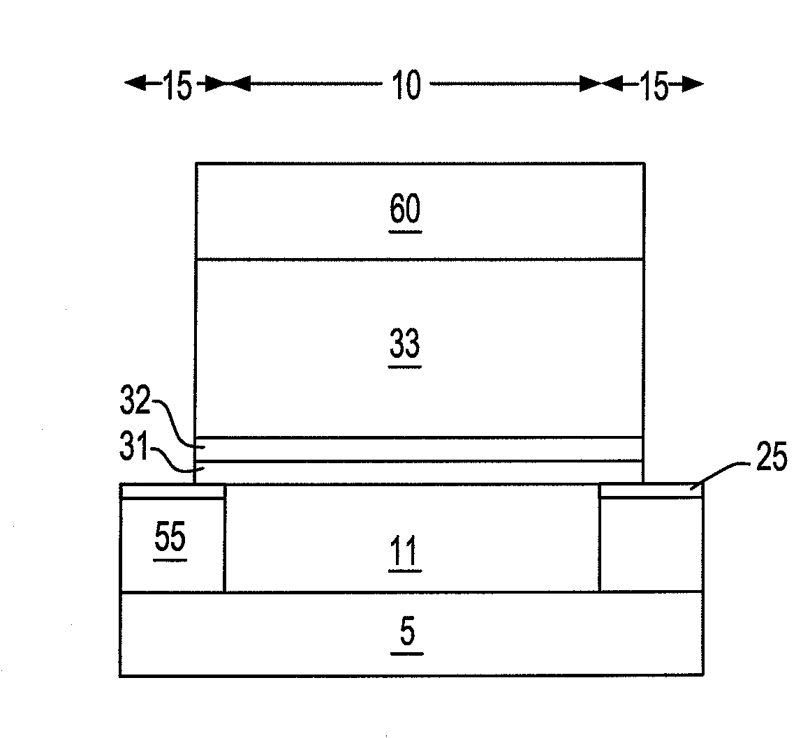
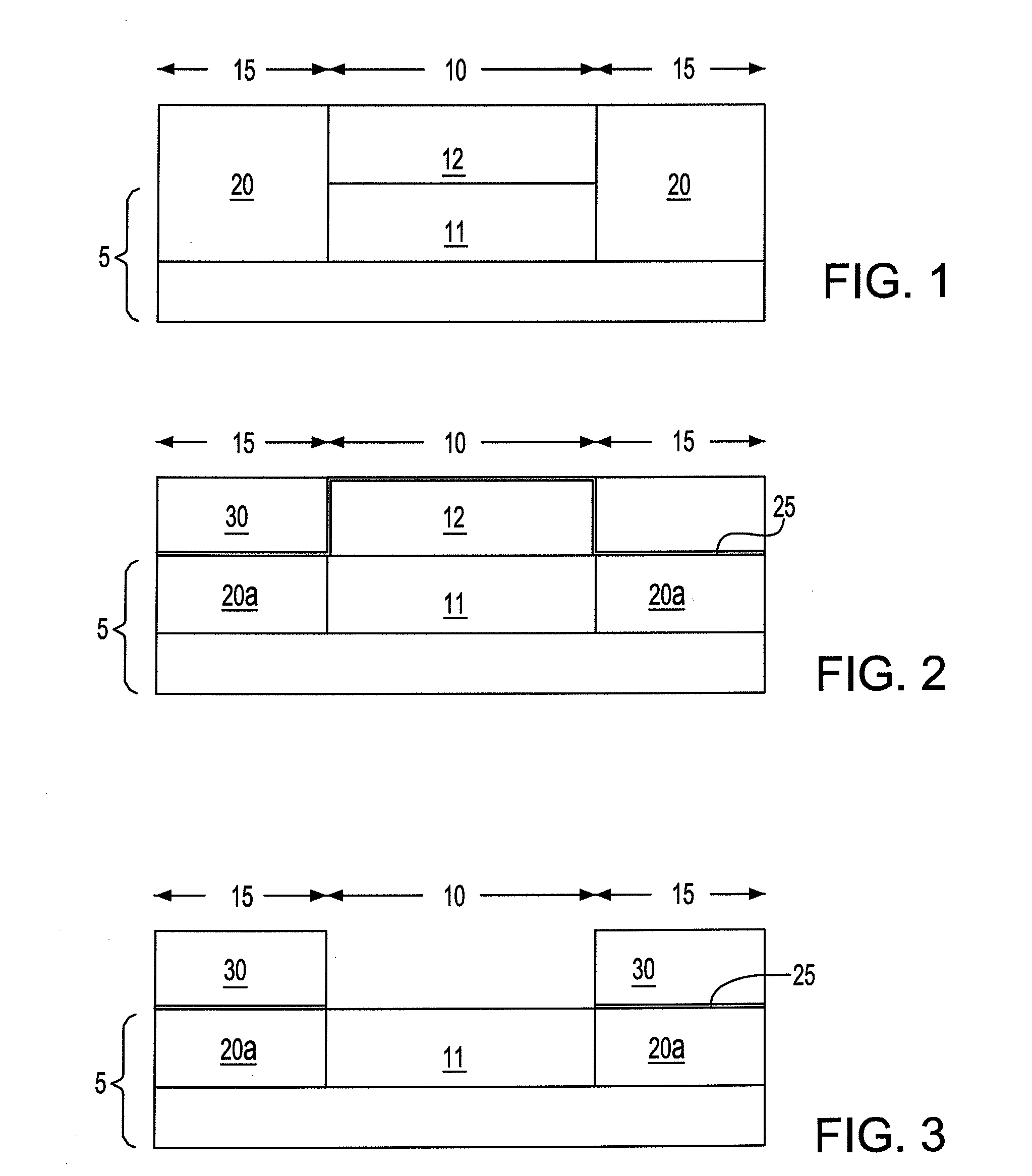
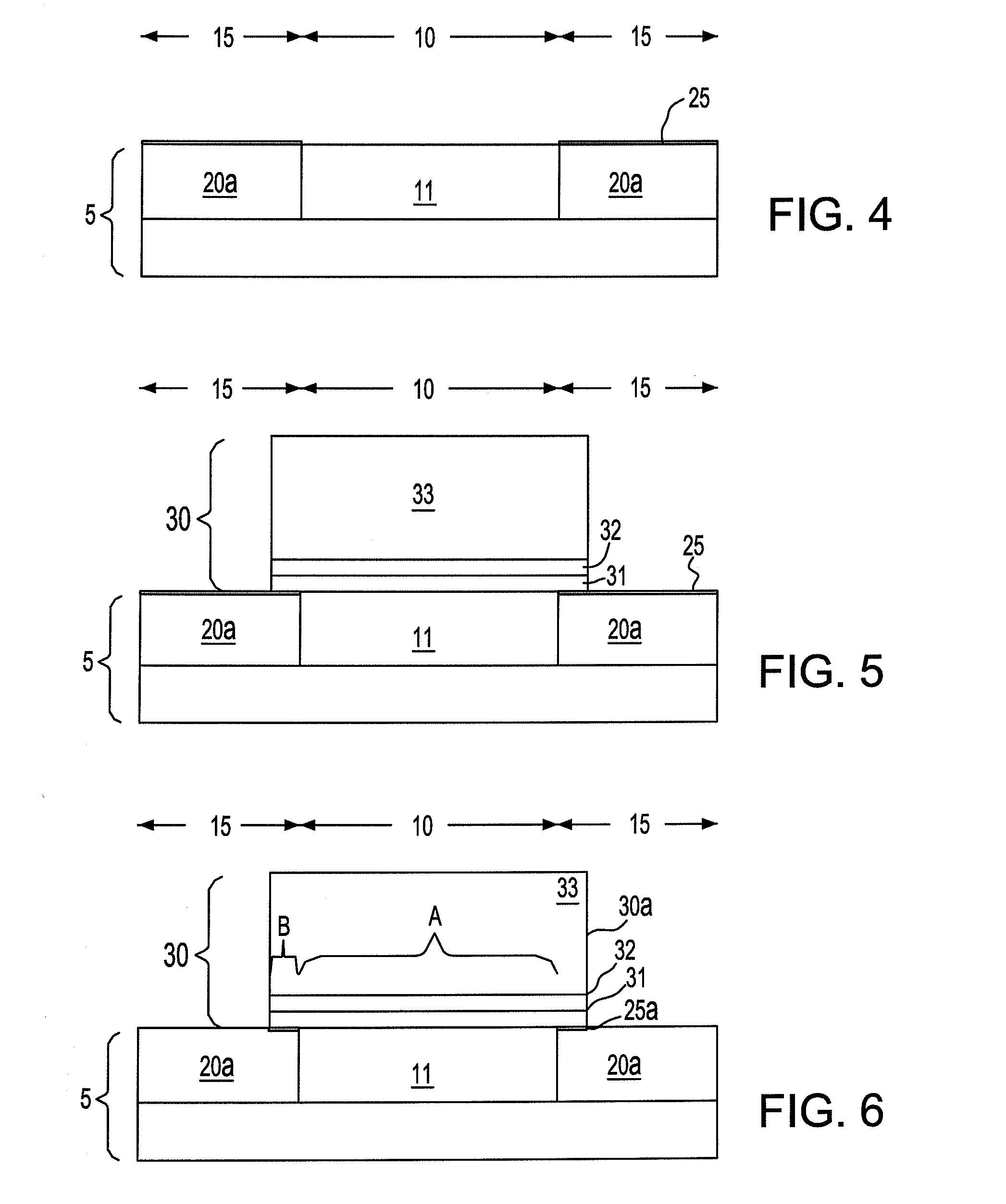
[0035]Detailed embodiments of the present invention are disclosed herein; however, it is to be understood that the disclosed embodiments are merely illustrative of the invention that may be embodied in various forms. In addition, each of the examples given in connection with the various embodiments of the invention are intended to be illustrative, and not restrictive. Further, the figures are not necessarily to scale, some features may be exaggerated to show details of particular components. Therefore, specific structural and functional details disclosed herein are not to be interpreted as limiting, but merely as a representative basis for teaching one skilled in the art to variously employ the present invention.
[0036]The embodiments of the present invention relate to novel methods and structures relating to gate structures in semiconducting devices. When describing the inventive methods and structures, the following terms have the following meanings, unless otherwise indicated.
[003...
PUM
 Abstract
Description
Claims
Application Information