Circuit board and manufacturing method thereof

Active Publication Date: 2009-10-08
UNIMICRON TECH CORP
View PDF7 Cites 0 Cited by
  • Summary
  • Abstract
  • Description
  • Claims
  • Application Information

AI Technical Summary

Benefits of technology

[0006]The present invention is directed to a circuit board and manufacturing method thereof, so as to achieve good signal propagation in the internal circuits of the circuit board.
[0014]In the present invention, the second circuit layer is, for example, a main circuit for transmitting electrical signals, and the first circuit layer is, for example, a shielding circuit. Therefore, when the electrical signals propagate on the main circuit, the shielding circuit may exert the shielding function, for effectively alleviating the electromagnetic interference between the main circuits, and thus the main circuits have a good signal transmission quality.

Problems solved by technology

However, since the technical requirement of the signal propagation frequency transmitting by the circuit layers becomes increasingly high, the electromagnetic interference and noises between any two circuit layers gradually aggravates.

Method used


Image

  • Circuit board and manufacturing method thereof
  • Circuit board and manufacturing method thereof
  • Circuit board and manufacturing method thereof

Examples


Embodiment Construction

[0019]Reference will now be made in detail to the present preferred embodiments of the invention, examples of which are illustrated in the accompanying drawings. Wherever possible, the same reference numbers are used in the drawings and the description to refer to the same or like parts.

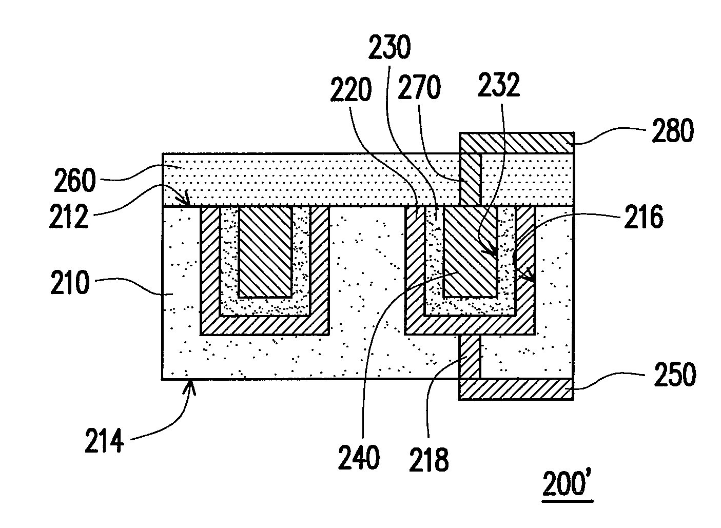
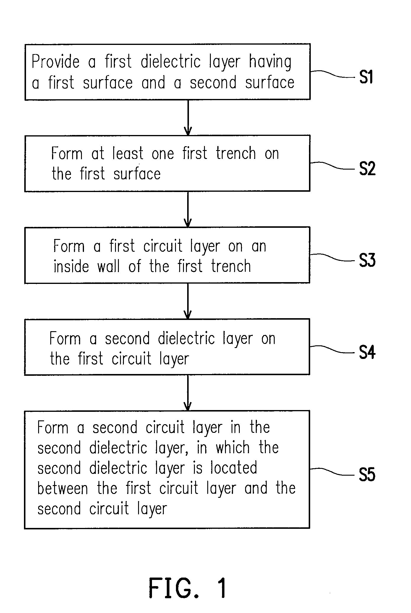
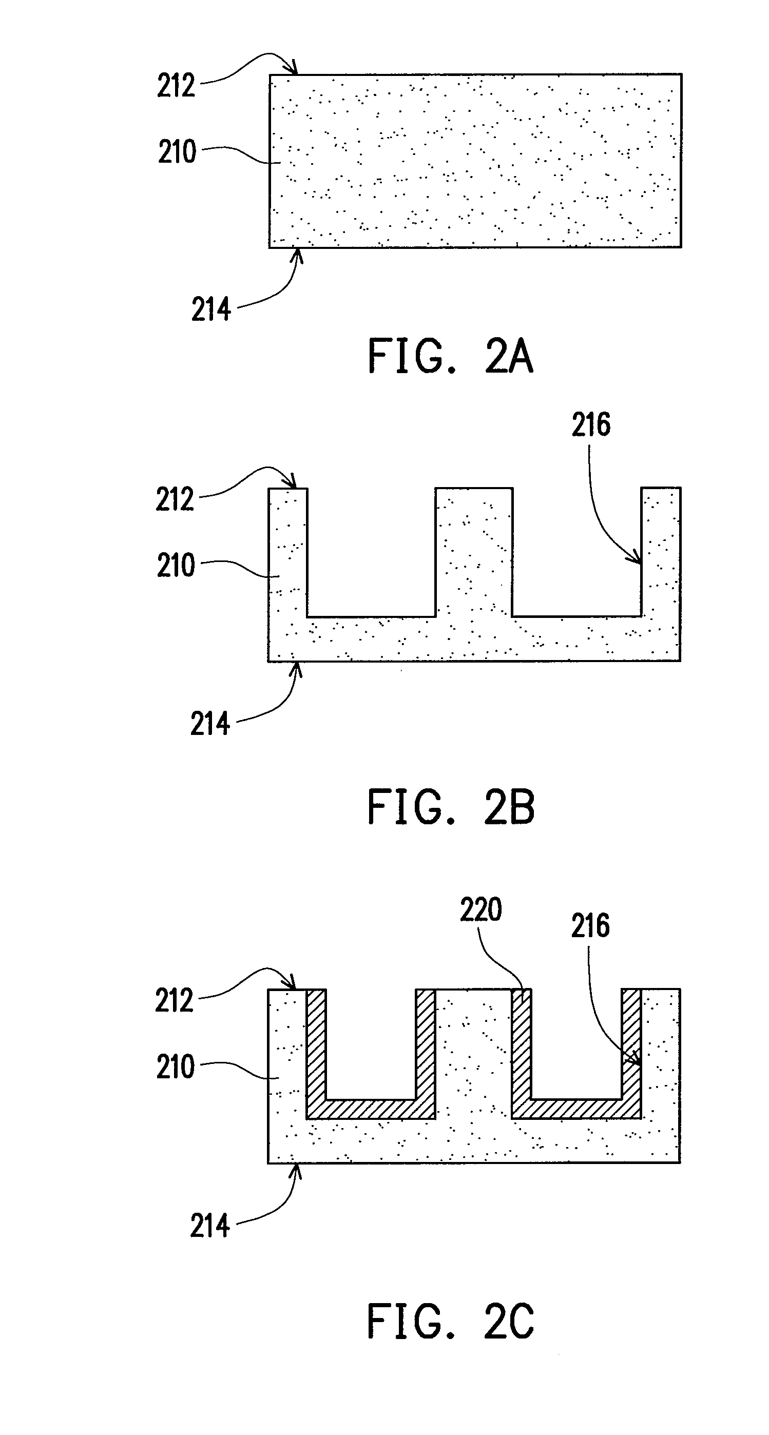
[0020]FIG. 1 is a schematic view of processes of manufacturing a circuit board according to an embodiment of the present invention. Referring to FIG. 1, in this embodiment, the manufacturing method of a circuit board includes the following steps. First, in Step S1, a first dielectric layer having a first surface and a second surface is provided. Then, in Step S2, at least one first trench is formed on the first surface. After that, in Step S3, a first circuit layer is formed on an inside wall of the first trench. Thereafter, in Step S4, a second dielectric layer is formed on first circuit layer. Then, in Step S5, a second circuit layer is formed in second dielectric layer. The second dielectric layer...


PUM

PropertyMeasurementUnit
Electrical conductoraaaaaaaaaa
Dielectric constantaaaaaaaaaa

Abstract

A circuit board including a first dielectric layer having a first surface and a second surface, a first circuit layer, a second dielectric layer, and a second circuit layer is provided. At least one trench is formed on the first surface, and the first circuit layer is formed on an inside wall of the trench. In addition, the second dielectric layer is disposed in the trench, and covers the first circuit layer. The second circuit layer is disposed in the trench, and the second dielectric layer is located between the first circuit layer and the second circuit layer. A manufacturing method of the circuit board is further provided.

Description

CROSS-REFERENCE TO RELATED APPLICATION[0001]This application claims the priority benefit of Taiwan application serial no. 97112489, filed on Apr. 7, 2008. The entirety of the above-mentioned patent application is hereby incorporated by reference herein and made a part of this specification.BACKGROUND OF THE INVENTION[0002]1. Field of the Invention[0003]The present invention generally relates to a circuit board and manufacturing method thereof, in particular, to a circuit board having electromagnetic shielding effect and a manufacturing method thereof.[0004]2. Description of Related Art[0005]Generally speaking, a circuit board for carrying or electrically connecting a plurality of electronic components is formed by alternately stacking a plurality of patterned conductive layers and a plurality of dielectric layers. The patterned circuit layers are defined by the copper foil after performing a photolithographic process. The dielectric layers are respectively disposed between two adjac...

Claims


Application Information

Patent Timeline
IPC IPC(8): H05K1/02H01R43/00
CPCH05K1/0219H05K1/0231H05K1/162Y10T29/49117H05K2201/09036H05K2201/09809H05K3/107
Inventor YU, CHENG-POYU, CHENG-HUNG
Owner UNIMICRON TECH CORP
Why Eureka
Try Eureka