Connections for electronic devices on double-sided circuit board

a technology of electronic devices and circuit boards, applied in the direction of printed circuit non-printed electric components association, sustainable manufacturing/processing, final product manufacturing, etc., can solve the problems of increasing the complexity and cost of the overall electronic structure, prohibitively expensive options, and detrimental to the integrity of the package signal

Active Publication Date: 2009-10-08
CYPRESS SEMICON CORP
View PDF30 Cites 68 Cited by
  • Summary
  • Abstract
  • Description
  • Claims
  • Application Information

AI Technical Summary

Problems solved by technology

This, along with the need for multiple layers for the circuit board 38, greatly increases the complexity and cost of the overall electronic structure.
However, present chip mask costs, even for only a partial mask set change,

Method used


Image

  • Connections for electronic devices on double-sided circuit board
  • Connections for electronic devices on double-sided circuit board
  • Connections for electronic devices on double-sided circuit board

Examples


Embodiment Construction

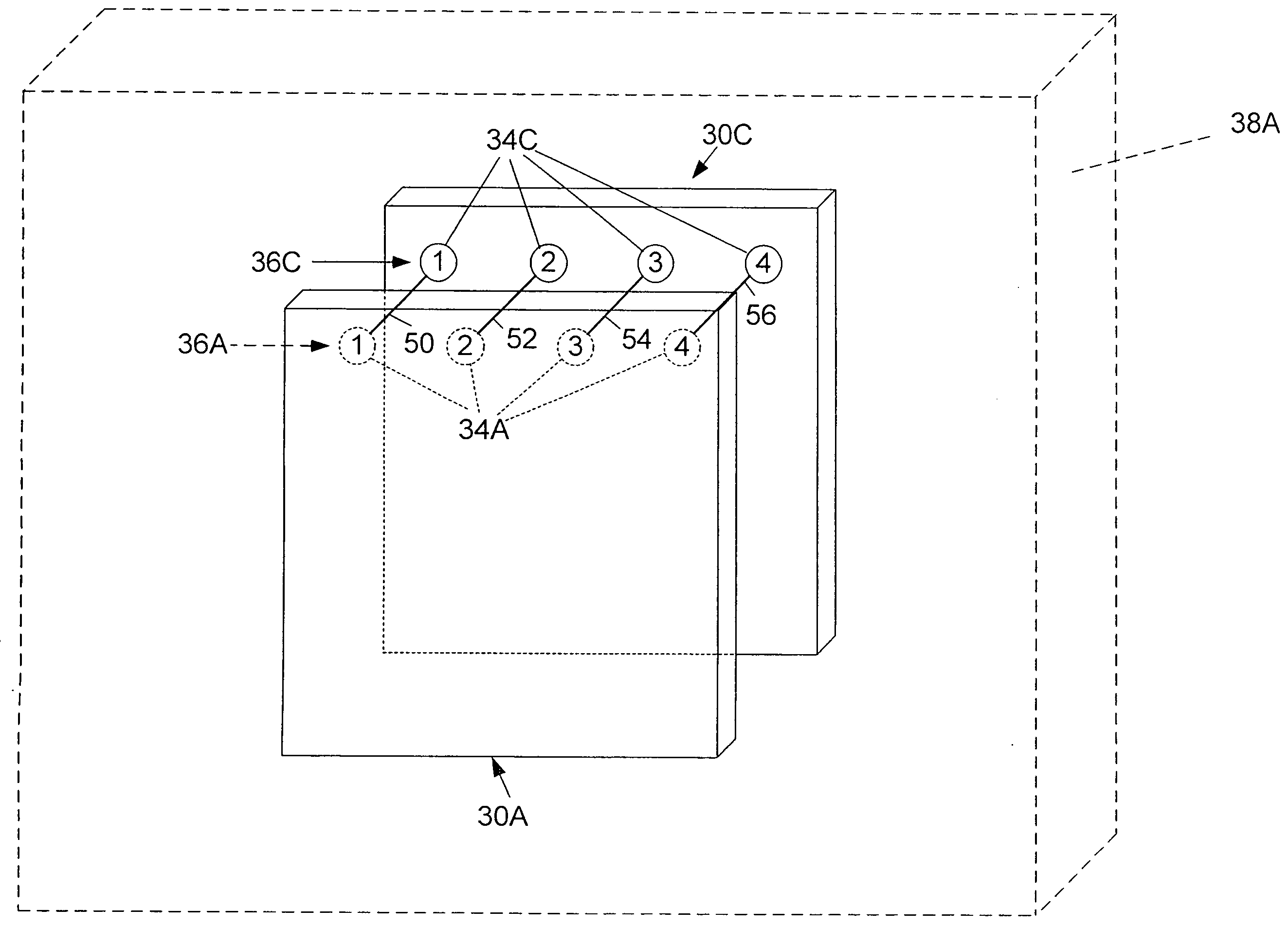
[0023]Reference is now made in detail to specific embodiments of the present invention which illustrate the best mode presently contemplated by the inventors for practicing the invention. FIGS. 5 and 6 illustrate packaged semiconductor devices. FIG. 6 illustrates a device identical to device 30A shown in FIG. 3 and device 30 in FIGS. 1 and 2. As such, the device 30A includes a ball grid array 32A on one side thereof (shown on the side of the device 30 facing away from the viewer of FIG. 6), with the number of balls of the array shown greatly reduced for clarity. The ball grid array 32A includes a plurality of conductive balls which make up contacts formed in rows. For example, the row 36A of contacts 34A includes contacts 34A-1, 34A-2, 34A-3, 34A-4 (reading from left to right in FIG. 6). The contacts 34A communicate with a semiconductor chip (not shown) inside the package, as is well known.

[0024]FIG. 5 illustrates a device 30C like device 30A shown in FIG. 3 and device 30 in FIGS. 1...


PUM


Abstract

In the present electronic structure, a substrate is provided in the form of a circuit board. First and second electronic devices are positioned on opposite sides of the circuit board, each having a plurality of contacts connected to the circuit board. Each of the contacts of the first device is connected to a contact of the second device by a connector though the circuit board. At least one of the contacts of the first device is connected to the contact of the second device which is most adjacent to that contact of the first device across the circuit board.

Description

BACKGROUND OF THE INVENTION[0001]1. Technical Field[0002]This invention relates generally to electronic devices, and more particularly, to an approach for connecting electronic devices on opposite sides of a circuit board.[0003]2. Background Art[0004]FIG. 1 illustrates an electronic device in the form of a packaged semiconductor device 30. The device 30 includes a ball grid array 32 on one side thereof (shown on the side of the device 30 facing the viewer of FIG. 1), with the number of balls of the array shown greatly reduced for clarity. The ball grid array includes a plurality of conductive balls which make up contacts formed in rows, patterns or other arrangements. In this embodiment, rows are depicted For example, the row 36 of contacts 34 includes contacts 34-4, 34-3, 34-2, 34-1 (reading from left to right in FIG. 1). The contacts 34 communicate with a semiconductor chip (not shown) inside the package, as is well known.[0005]FIG. 2 illustrates the device 30 of FIG. 1 rotated 18...

Claims


Application Information

Patent Timeline
IPC IPC(8): H05K1/18
CPCH01L23/50H01L23/5383H01L25/105H01L2225/06517H01L2225/06527H01L2225/06572H01L2225/107H05K1/181H05K2201/09227H05K2201/09481H05K2201/10545H05K2201/10734H01L2224/16225H01L2924/3011Y02P70/50
Inventor SHILLING, THOMAS H.SNIDER, TODDGRUPEN-SHEMANSKY, MELISSA
Owner CYPRESS SEMICON CORP
Why Eureka
Try Eureka