Semiconductor package having thermal stress canceller member

a technology of thermal stress canceller and semiconductor package, which is applied in the direction of semiconductor/solid-state device details, electrical apparatus, semiconductor devices, etc., can solve the problems of poor connection, potential connection defect, and possible warping of semiconductor package, and achieve the effect of reducing warping and virtually eliminating warping caused by thermal stress

Inactive Publication Date: 2009-10-08
RENESAS ELECTRONICS CORP
View PDF1 Cites 14 Cited by
  • Summary
  • Abstract
  • Description
  • Claims
  • Application Information

AI Technical Summary

Benefits of technology

[0012]The thermal stress canceller member cancels out the thermal stress caused by the difference in the thermal expansion rates between a package substrate and a mounting section including the first semiconductor chip and a first resin layer. The ex

Problems solved by technology

When there are curvatures such as warping in the semiconductor package, the gap between the pads on the wiring board and their corresponding external terminals becomes larger or similar effects occur, causing poor connections, and leading to potential connection defects.
Warping in semiconductor packages is caused mainly due to the many different materials making up the semiconductor package, and occurs due to the

Method used


Image

  • Semiconductor package having thermal stress canceller member
  • Semiconductor package having thermal stress canceller member
  • Semiconductor package having thermal stress canceller member

Examples


Embodiment Construction

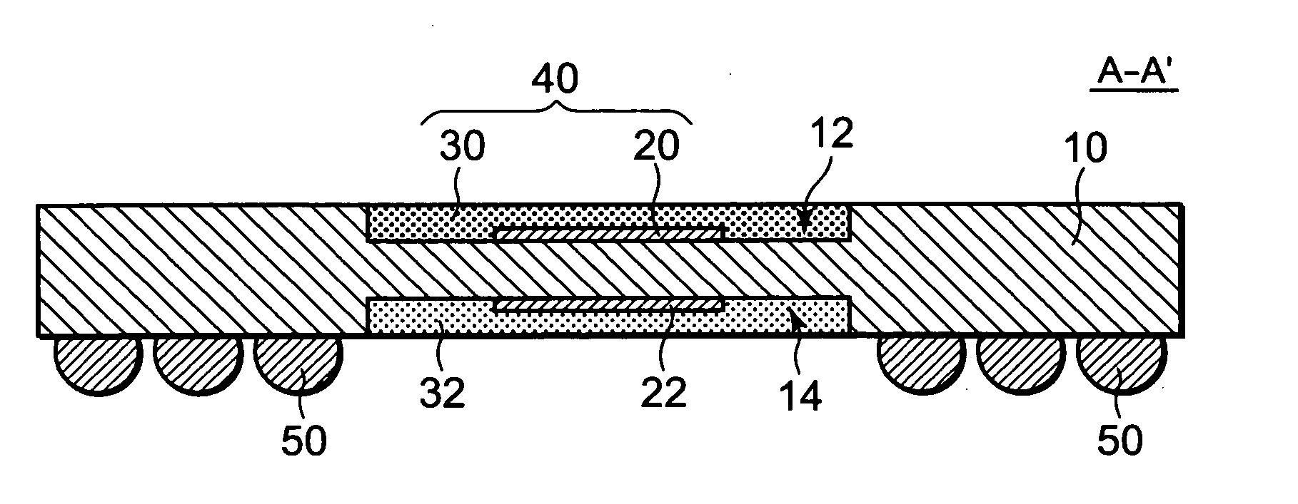
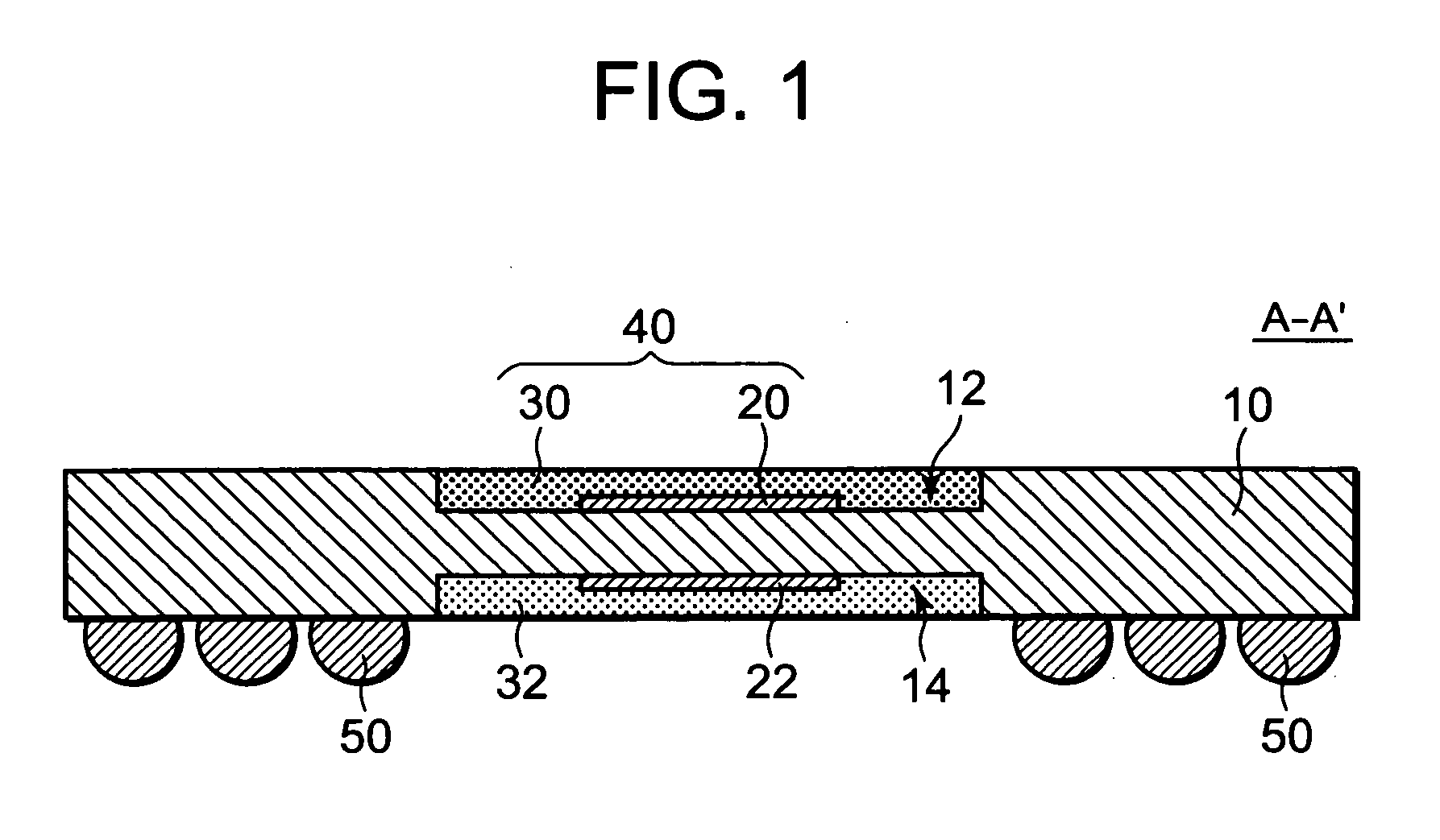
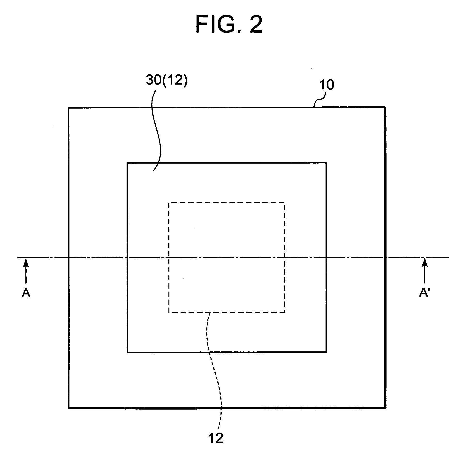
[0031]In the following exemplary embodiments, the semiconductor package includes a package substrate 10, a first cavity 12 formed on the package substrate 10, a first semiconductor chip 20, a first resin layer 30, and a thermal stress canceller member. The first cavity 12 is formed on the first main surface of the package substrate 10. The first semiconductor chip 20 is mounted on the bottom surface of the first cavity 12. The first resin layer 30 is filled into the first cavity 12. The thermal stress canceller member cancels out thermal stress caused by the difference in thermal expansion rates between the package substrate 10 and the mounting section 40 that includes the first semiconductor chip 20 and the first resin layer 30. The warping caused by thermal stress in the semiconductor package can therefore be suppressed. Moreover, warping caused by thermal stress can virtually be eliminated by adjusting items such as the configuration, the shape, and the material of the thermal ca...


PUM


Abstract

A semiconductor package includes a package-substrate, a first cavity formed on a first main surface of the package substrate, a first semiconductor chip mounted on the bottom surface of the first cavity, a first resin layer filled into the first cavity, and a thermal stress canceller member mounted on the package substrate for cancelling the thermal stress caused by the difference in the thermal expansion rates between the package substrate and mounting section including a first semiconductor chip and a first resin layer. The thermal stress canceller member may include a second cavity, a second resin layer filled into the second cavity, and a semiconductor chip.

Description

BACKGROUND OF THE INVENTION[0001]1. Field of the Invention[0002]The present invention relates to a semiconductor package where a semiconductor chip is mounted on a package substrate.[0003]2. Description of Related Art[0004]Electronic equipment and hand-held devices of various types are constantly being made more compact and lighter in weight, so the semiconductor packages used in those devices and equipment must also be reduced in size, be made lighter, and to a thinner profile. Moreover, there is a growing trend to increase the number of external terminals for data input / output on semiconductor packages in order to keep pace with increasingly sophisticated and higher performance electronic equipment and other devices. These circumstances have led to the widespread use of surface-mounted semiconductor packages containing many external terminals on one surface of the semiconductor package. This type of surface-mounted semiconductor package should be positioned in as level a state as ...

Claims


Application Information

Patent Timeline
IPC IPC(8): H01L23/34H01L23/00
CPCH01L23/367H01L23/3677H01L23/49816H01L23/49833H01L25/0652H01L25/0657H01L2225/06572H01L2924/0002H01L2225/06589H01L2924/12044H01L2924/15311H01L2924/00
Inventor YOSHIDA, YUICHI
Owner RENESAS ELECTRONICS CORP
Why Eureka
Try Eureka