EL display panel and electronic apparatus

a display panel and electronic technology, applied in the field of electroluminescence display panels, can solve the problems of affecting the accuracy of mobility correction and changing so as to reduce the amount of internal scattered light incident on the channel layer of sampling transistors, stabilize the operating point of mobility correction, and minimize the influence of internal scattered ligh

Inactive Publication Date: 2009-10-22
SONY CORP
View PDF8 Cites 69 Cited by
  • Summary
  • Abstract
  • Description
  • Claims
  • Application Information

AI Technical Summary

Benefits of technology

[0060]This means that the light amount of internal scattered light incident on the channel layer of the sampling transistor can be decreased. That is, the influence of the internal scattered light can be minimized although it may be difficult to completely eliminate the influence. Thus, the operating point in mobility correction can be stabilized.

Problems solved by technology

However, change in the threshold voltage Vth of the sampling transistor T1 (i.e. change in the on-period thereof) causes change in the operating point of the mobility correction for the drive transistor T2 and thus affects the accuracy of the mobility correction.
However, part of the scattered light is often repeatedly reflected inside the panel.
That is, it leads to change in the operating point of the mobility correction.

Method used


Image

  • EL display panel and electronic apparatus
  • EL display panel and electronic apparatus
  • EL display panel and electronic apparatus

Examples


first form example

(B) First Form Example

(B-1) System Configuration

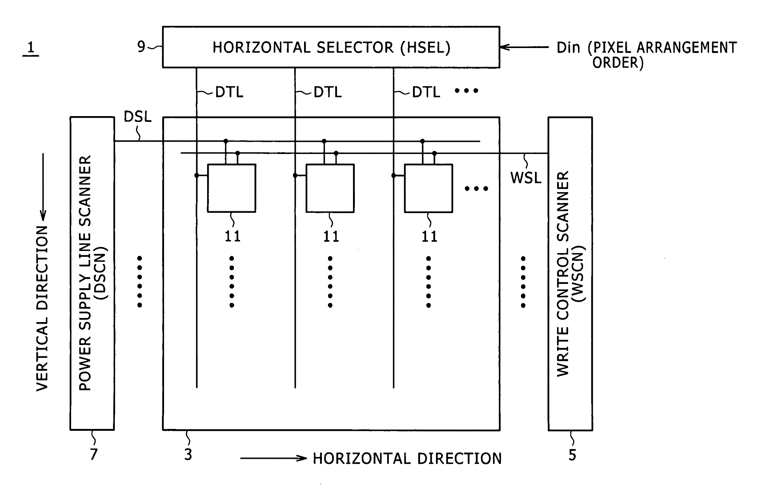
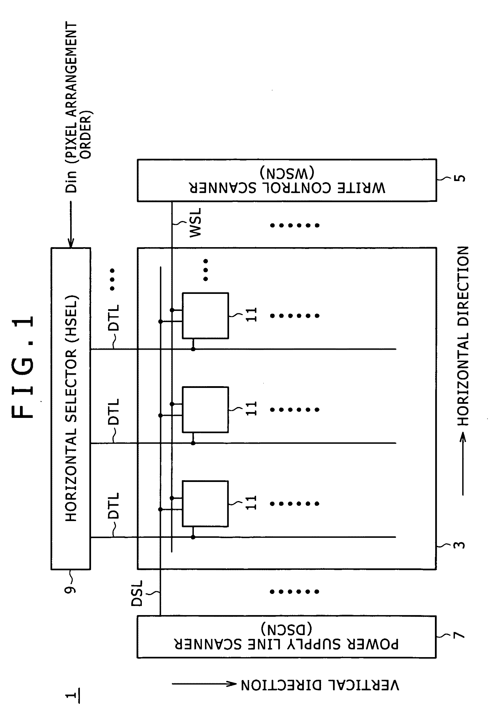
[0100]FIG. 12 shows a system configuration example of an organic EL panel 71 according to a form example of the present invention. The same components in FIG. 12 as those in FIG. 1 are given the same numerals.

[0101]The organic EL panel 71 shown in FIG. 12 includes a pixel array part 73, and a write control scanner 75, a power supply line scanner 7, and a horizontal selector 9 as drive circuits for the pixel array part 73.

(1) Configuration of Pixel Array Part

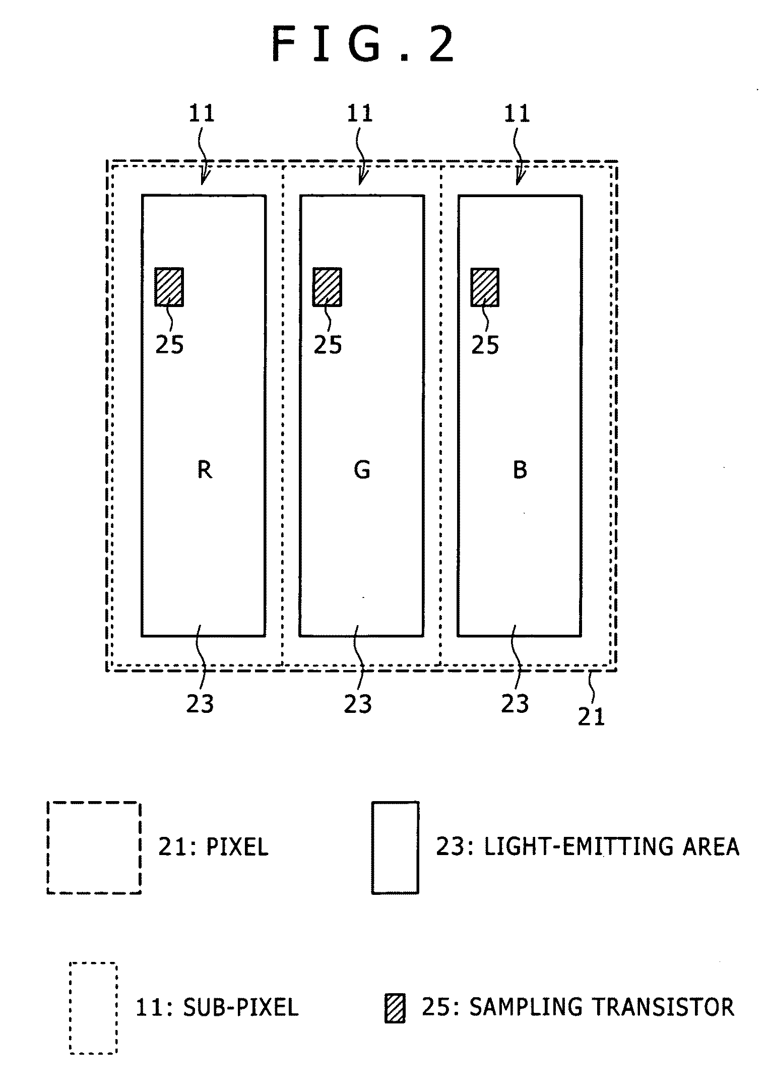
[0102]In the pixel array part 73, sub-pixels 11 corresponding to red (R) pixels, green (G) pixels, and blue (B) pixels are arranged in a matrix. FIG. 13 shows the connection relationship between the pixel circuit corresponding to the sub-pixel 11 and the above-described respective drive circuits.

[0103]The electric configuration of the pixel circuit in this form example is the same as that shown in FIG. 3. Specifically, this pixel circuit includes a sampling transistor T1, a drive tr...


PUM


Abstract

Disclosed herein is an electroluminescence display panel including pixel circuits corresponding to an active-matrix drive system, the electroluminescence display panel including a structure configured to include first light-emitting areas corresponding to an emission color that is strongest in a characteristic of changing a threshold voltage of a thin film transistor and second light-emitting areas that correspond to another emission color and are each disposed between the first light-emitting areas, wherein a sampling transistor in each of the pixel circuits for driving the second light-emitting areas is disposed in an area corresponding to a range of one fourth to three fourths of a length from a peripheral edge of one of two first light-emitting areas that are adjacent to each other with intermediary of the second light-emitting area of the sampling transistor to a peripheral edge of the other of the two first light-emitting areas.

Description

CROSS REFERENCES TO RELATED APPLICATIONS[0001]The present invention contains subject matter related to Japanese Patent Application JP 2008-074774 filed in the Japan Patent Office on Mar. 23, 2008, the entire contents of which being incorporated herein by reference.BACKGROUND OF THE INVENTION[0002]1. Field of the Invention[0003]The invention to be described in this specification relates to an EL (electroluminescence) display panel whose driving is controlled based on an active-matrix drive system. The invention to be proposed by this specification also has a mode as various kinds of electronic apparatus including an EL display panel.[0004]2. Description of the Related Art[0005]FIG. 1 shows a configuration example of a circuit block used in an active-matrix driven organic EL panel. An organic EL panel 1 shown in FIG. 1 includes a pixel array part 3, and a write control scanner 5, a power supply line scanner 7, and a horizontal selector 9 as drive circuits for the pixel array part 3.[0...

Claims


Application Information

Patent Timeline
Patent Type & Authority Applications(United States)
IPC IPC(8): G09G3/30H05B44/00
CPCH01L27/3211H01L27/3276H01L27/3262H01L27/3213H10K59/351H10K59/353H10K59/1213H10K59/131H01L23/49838H10K59/35H10K59/12
Inventor YAMASHITA, JUNICHIYAMAMOTO, TETSUROUCHINO, KATSUHIDE
Owner SONY CORP
Why Eureka
Try Eureka