

Holographic scatterometer
a scatterometer and holographic technology, applied in the field of scatterometers, can solve problems such as interference of test ligh
- Summary
- Abstract
- Description
- Claims
- Application Information
AI Technical Summary
Problems solved by technology
Method used
Image

Examples
Embodiment Construction
[0001]1. Field of the Invention
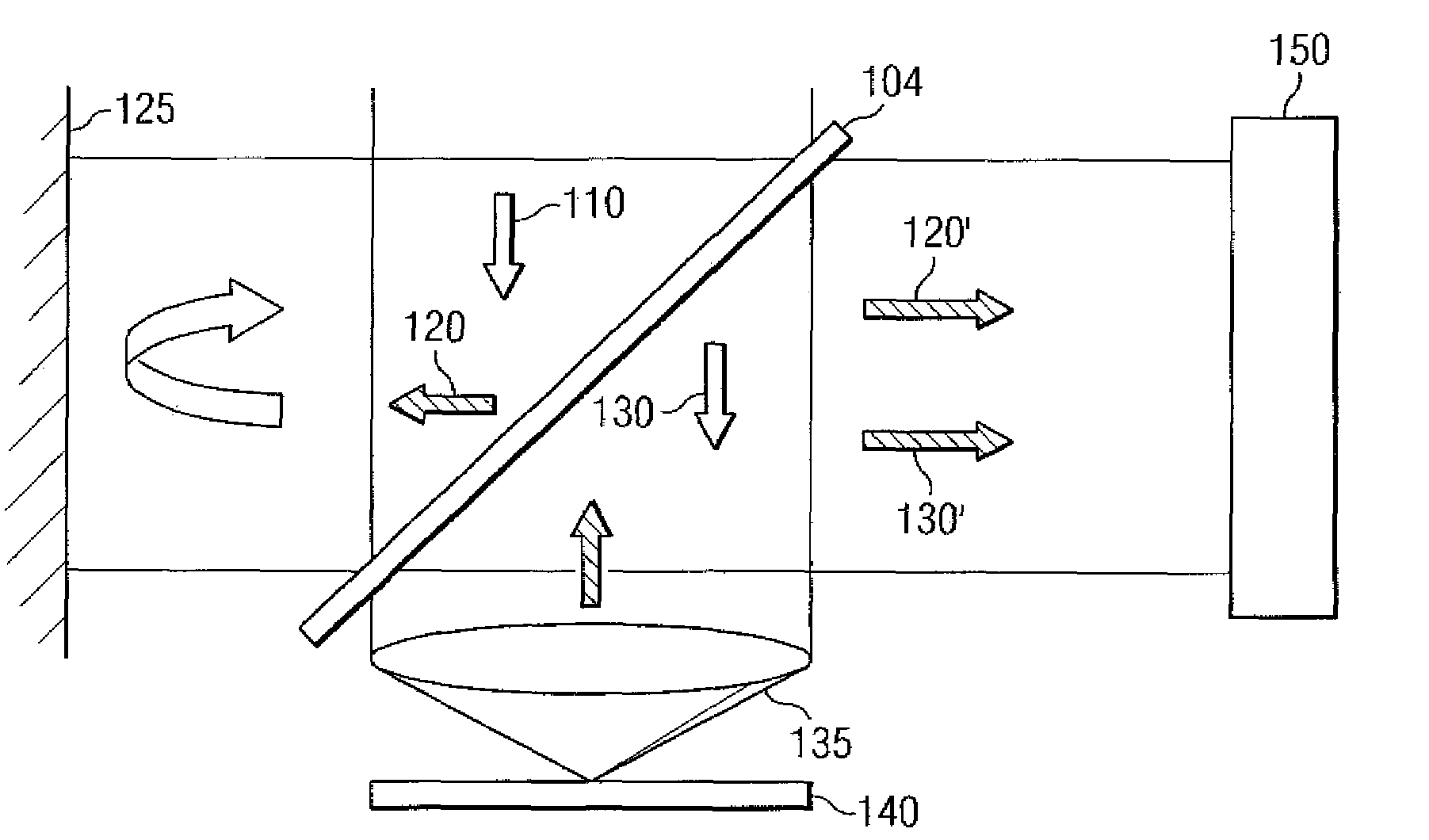
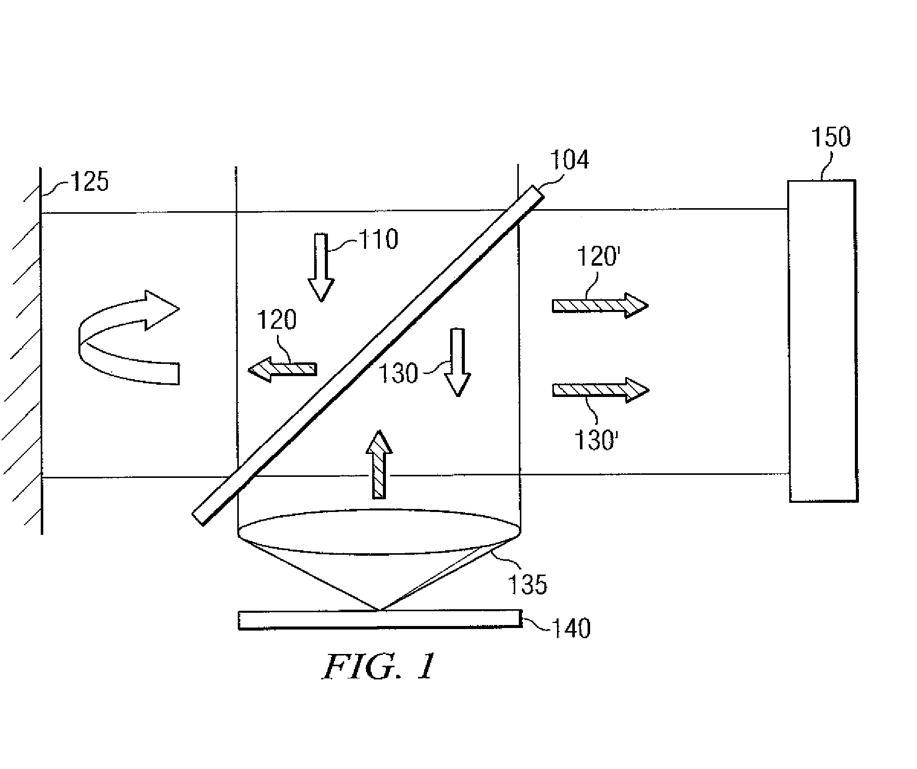
[0002]This invention generally relates to a scatterometry system and, more particularly, to a holographic scatterometry system
[0003]2. Background of the Invention
[0004]Over the past several years, there has been considerable interest in using optical scatterometry (i.e., optical diffraction) to perform measurements associated with semiconductor fabrication. One area of great interest has been the critical dimension (CD) measurements of two-dimensional structures (e.g., line gratings) and three-dimensional structures (e.g., patterns of vias or mesas) included in integrated circuits. Scatterometry measurements have also been proposed for monitoring etching, planarity of a polished layer, control of gate electrode profiles, film stack fault detection, stepper control, deposition process control and resist thickness control.
[0005]Various optical techniques have been used to perform optical scatterometry. These techniques include spectral ellipsometry (i.e....
PUM
 Abstract
Description
Claims
Application Information