Switch structures for use on printed circuit boards

a technology of printed circuit boards and switches, applied in the direction of emergency connections, contact forms, electrical apparatus construction details, etc., can solve the problems of unavoidable subjecting pcb contacts, pcb contacts to the possibility of corrosion, and hard gold plating can be expensive and/or difficult, etc., to achieve easy and cheaper operation, small and simple, and easy to apply

Active Publication Date: 2009-10-29
APPLE INC
View PDF8 Cites 22 Cited by
  • Summary
  • Abstract
  • Description
  • Claims
  • Application Information

AI Technical Summary

Benefits of technology

[0006]In accordance with certain other possible aspects of the invention, a PCB structure may include a main PCB structure having an electrical contact area on one of its main surfaces, a secondary PCB structure having first and second electrically connected electrical contacts disposed, respectively, on its two main surfaces, and anistropic conductive adhesive (“ACA”) for physically and electrically connecting the second contact and the contact area. The contact area does not need to be abrasion or corrosion resistant because it is covered by the ACA and the secondary PCB structure. The contact area can therefore have only an immersion gold covering, which is relatively easy to apply (although it is not particularly abrasion or corrosion resistant). Only the contacts on the secondary PCB structure (especially the more exposed first contact) need such abrasion and / or corrosion resistance (e.g., by being plated with hard gold). However, such hard gold plating is easier and cheaper to perform on the secondary PCB structure than on the main PCB structure because the secondary structure can be smaller and simpler than the main structure, and because the secondary structure can be fabricated separately from the main structure prior to being joined to the main structure by the ACA.

Problems solved by technology

Switches with a moving part or parts (e.g., dome switches) unavoidably subject PCB contacts like those mentioned above to abrasion each time the switch is operated.
This exposes the PCB contacts to the possibility of corrosion.
Hard gold plating can be expensive and / or difficult when an entire PCB must be subjected to such processing.

Method used


Image

  • Switch structures for use on printed circuit boards
  • Switch structures for use on printed circuit boards
  • Switch structures for use on printed circuit boards

Examples


Embodiment Construction

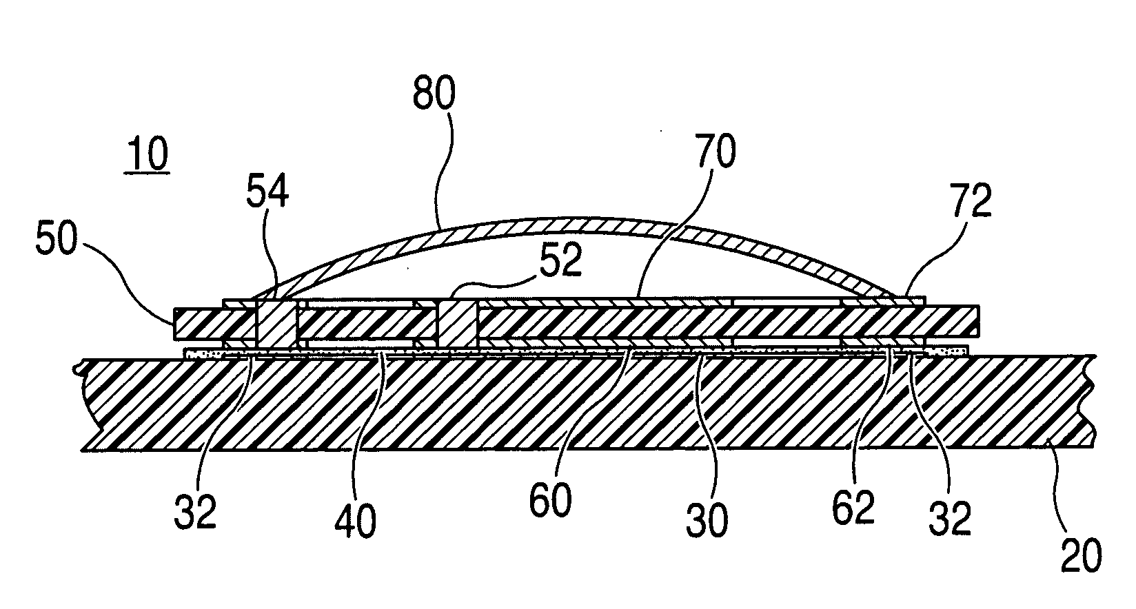
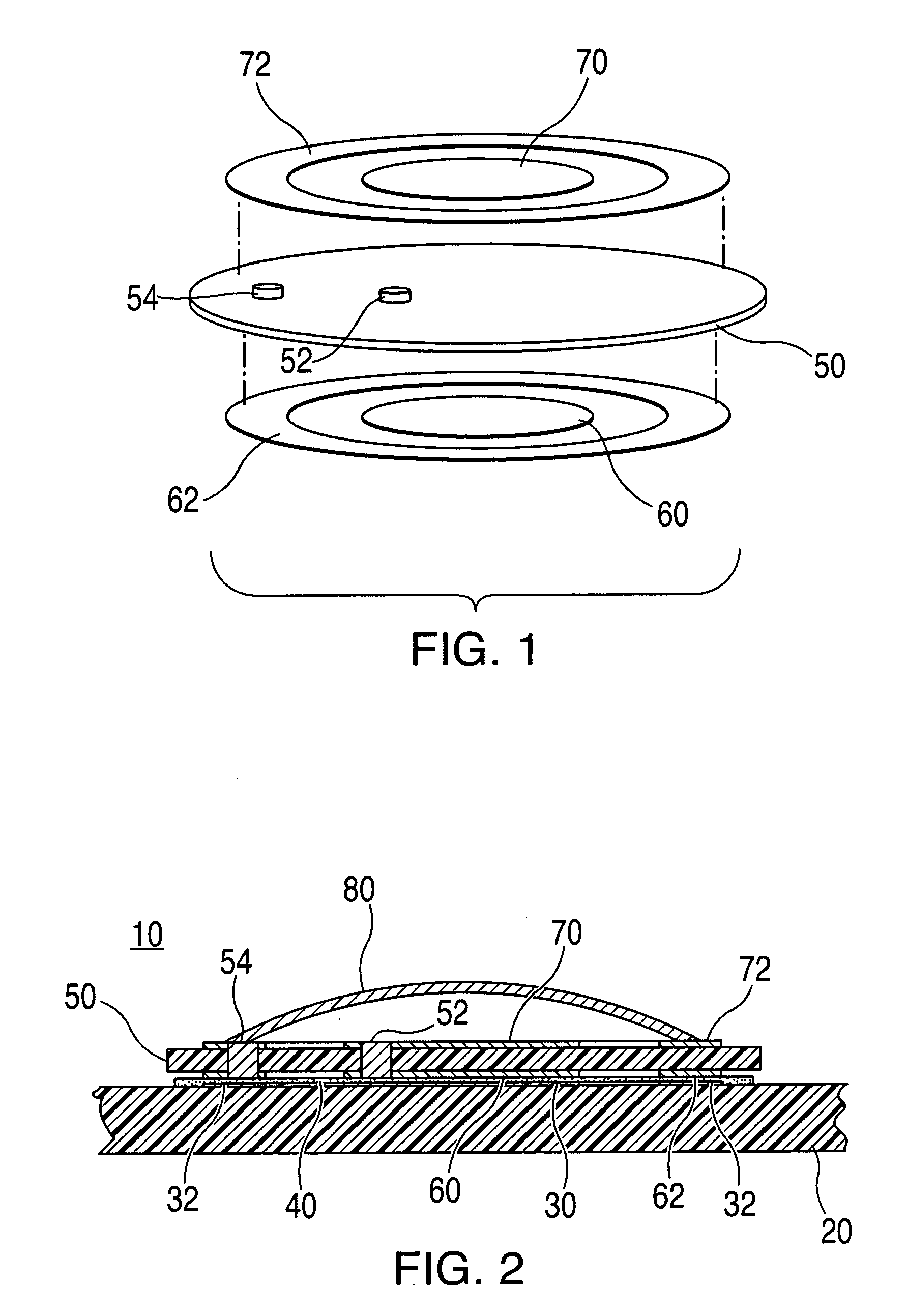
[0018]A cross section of an illustrative embodiment of a dome switch 10 in accordance with the invention is shown in FIG. 2, and several components of switch 10 are shown in an exploded perspective view in FIG. 1. Dome switch 10 is mounted on one of the two main or primary planar surfaces of main PCB 20, which can be conventional and which can extend away from dome switch 10 to include (or at least support and interconnect) any desired amounts and kinds of other circuitry.

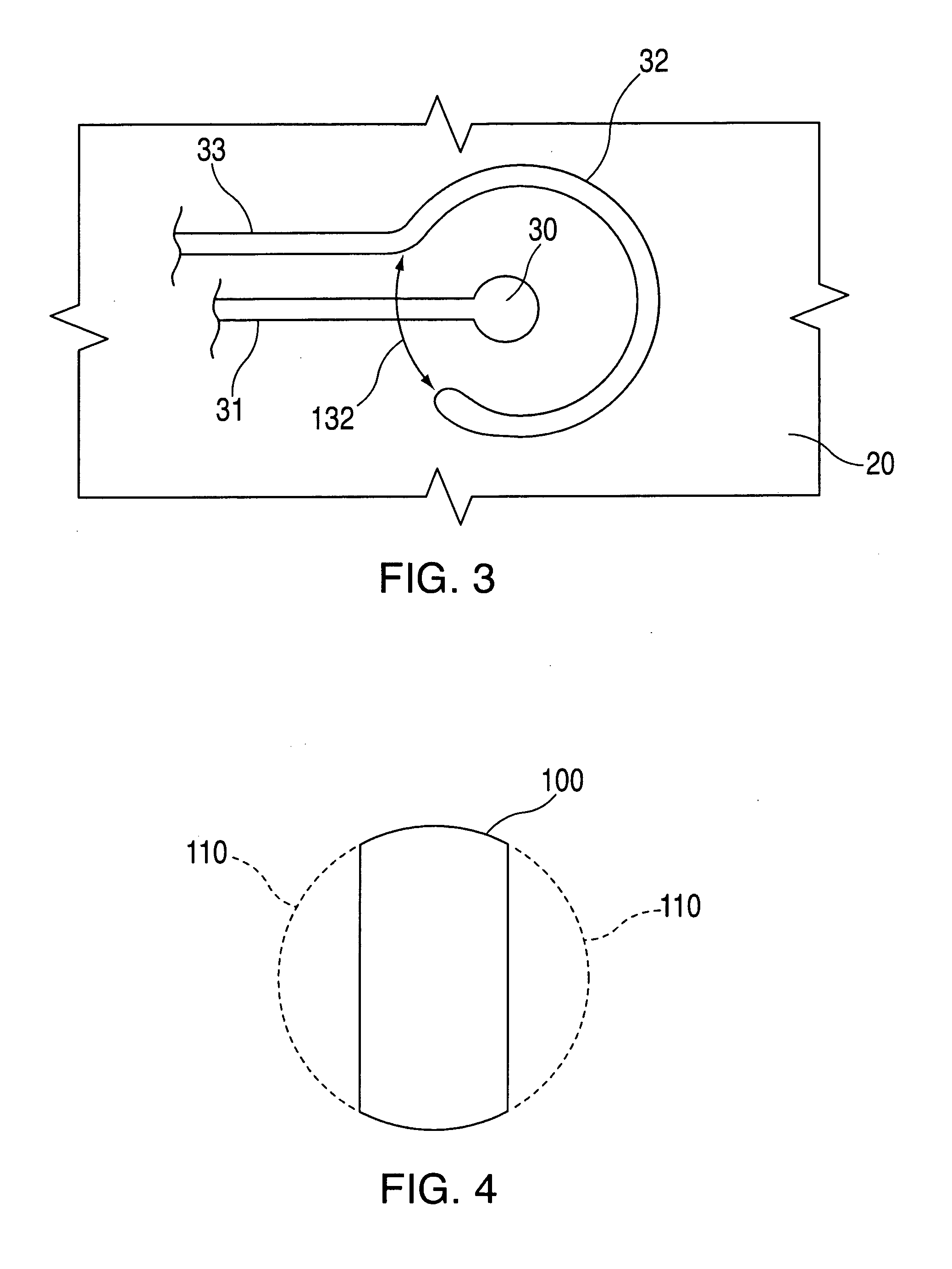
[0019]As shown in FIG. 2, the structure of dome switch 10 includes a circular inner contact 30 deposited on the upper main surface of PCB 20. For example, contact 30 may be formed from PCB electrical circuit trace material coated with immersion gold. Inner contact 30 is surrounded by ring-shaped outer contact 32, which is also deposited on the upper main surface of PCB 20 with some spacing or separation from all parts of inner contact 30. There is therefore normally no electrical connection between contacts 30 and ...


PUM


Abstract

An electrical contact area on a printed circuit board (“PCB”), that would otherwise be subject to abrasion and possibly also corrosion, can be protected by covering it with another, more durable contact structure that is bonded to the first-mentioned contact area using an anistropic conductive adhesive (“ACA”). The more durable contact structure may include a member of PCB material or the like with electrically connected electrical contacts on its upper and lower surfaces. At least the upper one of these contacts (which is exposed for the service that involves possible abrasion and / or corrosion) may be given high durability by plating it with hard gold. The lower of these contacts is adhered to the main PCB via the above-mentioned ACA.

Description

BACKGROUND OF THE INVENTION[0001]This invention relates to printed circuit boards, and more particularly to structures that can be used on printed circuit boards (“PCBs”) to facilitate the provision of electrical switches on such boards.[0002]PCBs are frequently constructed so that they can include one or more manually operable electrical switches. An example of such a switch is a so-called dome switch. A dome switch typically includes a circular metal disc that is resiliently biased to form a small dome above a surface of the PCB. The circular outer edge of the disc bears on a ring-shaped outer contact on the surface of the PCB. Another contact (the inner contact) is inside the outer contact on the PCB surface and under the center of (but not normally in contact with) the above-mentioned metal disc. The inner contact is spaced from all parts of the outer contact. The inner contact is therefore not normally in electrical contact with the outer contact. However, the center of the abo...

Claims


Application Information

Patent Timeline
Patent Type & Authority Applications(United States)
IPC IPC(8): H01H13/14H05K1/09
CPCH01H13/48H01H13/7006H01H13/78H01H13/785H01H2201/024H01H2201/03H05K2201/10053H01H2205/016H01H2207/008H01H2207/014H05K1/141H05K3/323H01H2203/038
Inventor ROTHKOPF, FLETCHER R.DABOV, TEODORDINH, RICHARD HUNG MINHSUN, JUNROSENBLATT, MICHAEL
Owner APPLE INC
Why Eureka
Try Eureka