Laser processing apparatus

a technology of laser processing and processing chamber, which is applied in the direction of manufacturing tools, instruments, welding/soldering/cutting articles, etc., can solve the problems of inability to detect the height of the front side of the workpiece in the case, the thickness and the depth of the laser processing groove cannot be uniformly measured

Active Publication Date: 2009-10-29
DISCO CORP
View PDF3 Cites 54 Cited by
  • Summary
  • Abstract
  • Description
  • Claims
  • Application Information

AI Technical Summary

Benefits of technology

[0012]It is therefore an object of the present invention to provide a laser processing apparatus which can detect the height of a workpiece held on a chuck table and follow the focal position of a processing laser beam even when the workpiece is formed of a transparent material.
[0015]As described above, the focusing means for focusing the processing laser beam and the detecting laser beam includes the objective lens for focusing the processing laser beam and the detecting laser beam and the window lens for focusing the detecting laser beam without focusing the processing laser beam. Thus, the detecting laser beam having the annular spot shape to be applied to the workpiece is focused by the objective lens and the window lens. Accordingly, the NA of the focusing lens can be increased, so that the ratio in size between the annular spot shape reflected on the upper surface of the workpiece and the annular spot shape reflected on the lower surface of the workpiece can be increased. As a result, the reflected light having the annular spot shape reflected on the lower surface of the workpiece can be reliably blocked by the pinhole mask. Accordingly, it is possible to detect the height of the workpiece held on the chuck table and follow the focal position of the processing laser beam even when the workpiece is formed of a transparent material.

Problems solved by technology

However, the wafer has undulations, causing variations in thickness.
As a result, the focal point of the laser beam applied to the wafer cannot be set on the subject surface of the wafer, so that a laser processed groove having a uniform depth cannot be formed along each street.
Thus, according to the height detecting means disclosed in the above publication, the height of the front side of the workpiece cannot be detected in the case that the workpiece is formed of a transparent material.
That is, it is impossible to detect the height of the workpiece by using the detecting laser beam and simultaneously follow the focal position of the processing laser beam.

Method used


Image

  • Laser processing apparatus
  • Laser processing apparatus
  • Laser processing apparatus

Examples


Embodiment Construction

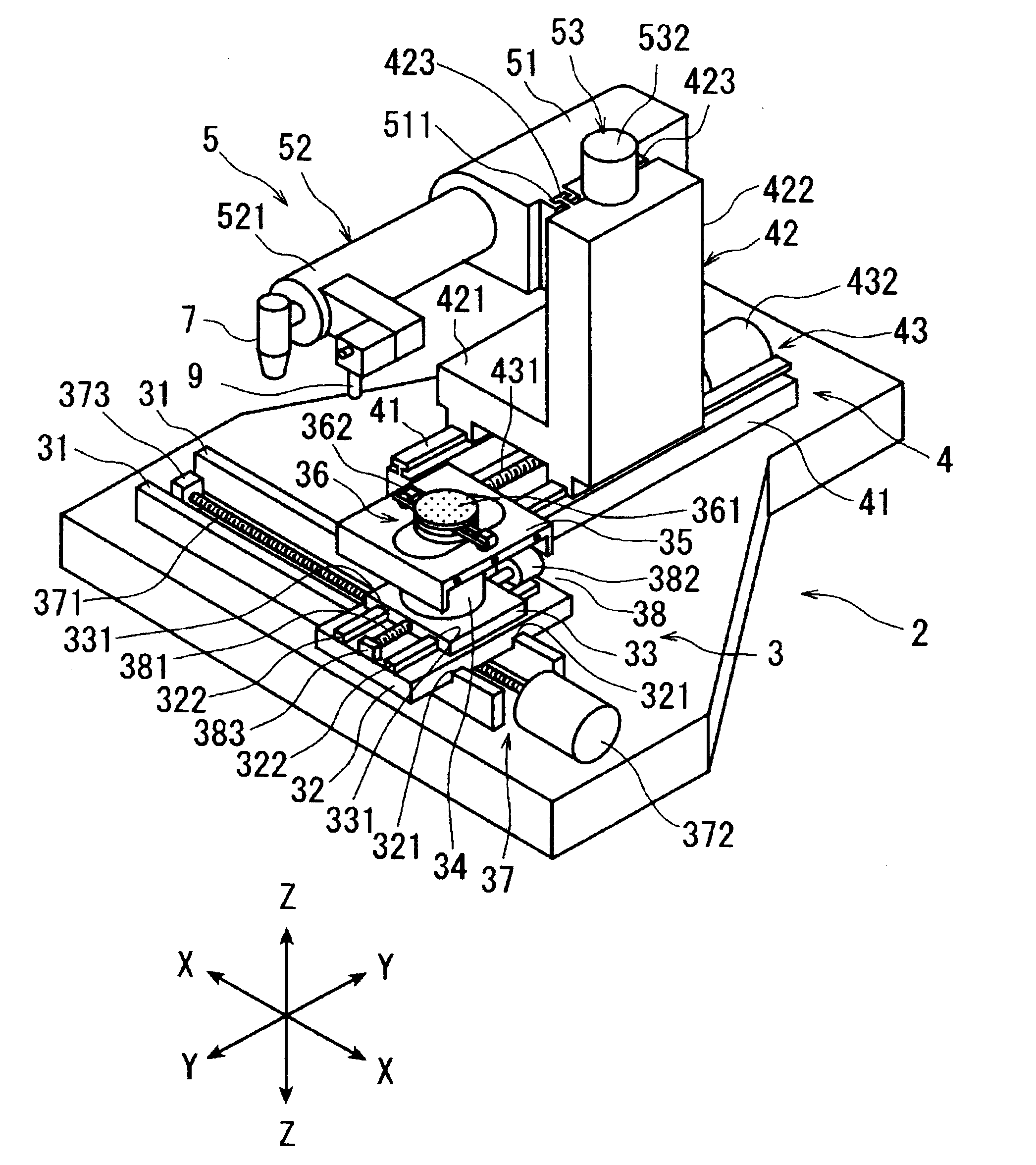
[0032]There will now be described a preferred embodiment of the laser processing apparatus according to the present invention with reference to the attached drawings. FIG. 1 is a perspective view of a laser processing apparatus according to a preferred embodiment of the present invention. The laser processing apparatus shown in FIG. 1 includes a stationary base 2, a chuck table mechanism 3 for holding a workpiece, the chuck table mechanism 3 being provided on the stationary base 2 so as to be movable in a feeding direction (X direction) shown by an arrow X, a laser beam applying unit supporting mechanism 4 provided on the stationary base 2 so as to be movable in an indexing direction (Y direction) shown by an arrow Y perpendicular to the feeding direction (X direction) shown by the arrow X mentioned above, and a laser beam applying unit 5 provided on the laser beam applying unit supporting mechanism 4 so as to be movable in a direction (Z direction) shown by an arrow Z.

[0033]The chu...


PUM

PropertyMeasurementUnit
absorption wavelengthaaaaaaaaaa
sizeaaaaaaaaaa
wavelengthaaaaaaaaaa

Abstract

A laser processing apparatus including a height detecting device for detecting the height of a workpiece held on a chuck table. The height detecting device includes an annular spot forming unit for forming the spot shape of a detecting laser beam into an annular spot shape, a pinhole mask for passing the reflected light reflected on the upper surface of the workpiece held on the chuck table, but blocking the reflected light reflected on the lower surface of the workpiece, and a reflected light analyzing unit for analyzing the reflected light passed through the pinhole mask and transmitting the result of analyzation to a control unit. The laser processing apparatus further includes a focusing unit having an objective lens for focusing a processing laser beam having a circular spot shape and the detecting laser beam having the annular spot shape and a window lens for focusing the detecting laser beam focused by the objective lens without focusing the processing laser beam.

Description

BACKGROUND OF THE INVENTION[0001]1. Field of the Invention[0002]The present invention relates to a laser processing apparatus for performing laser processing along streets formed on a wafer such as a semiconductor wafer.[0003]2. Description of the Related Art[0004]In a semiconductor device fabrication process, the front side of a substantially disk-shaped semiconductor wafer is formed with a plurality of crossing division lines called streets to thereby define a plurality of partitioned regions arranged like a matrix, and a plurality of devices such as ICs (Integrated Circuit) and LSIs (Large Scale Integration) are formed in these partitioned regions. The semiconductor wafer is cut along these streets to divide the partitioned regions, thus fabricating the individual devices. Further, an optical device wafer is fabricated by layering photodetectors such as photodiodes or light emitting devices such as laser diodes on the front side of a sapphire substrate. The optical device wafer i...

Claims


Application Information

Patent Timeline
Patent Type & Authority Applications(United States)
IPC IPC(8): B23K26/38B23K26/02B23K26/00G01B11/00
CPCB23K26/046B23K26/0807H01L21/78B23K26/367B23K26/4075B23K26/0853B23K26/082B23K26/364B23K26/40B23K2103/50
Inventor SAWABE, TAIKINOMARU, KEIJI
Owner DISCO CORP
Why Eureka
Try Eureka