Exposure apparatus and device fabrication method

a technology of exposure apparatus and fabrication method, which is applied in the direction of photomechanical apparatus, printing, instruments, etc., can solve the problems of increasing the number of lenses, and prone to humidity of the photodiode, so as to increase the na of exposure light

Inactive Publication Date: 2008-06-26
CANON KK
View PDF1 Cites 2 Cited by
  • Summary
  • Abstract
  • Description
  • Claims
  • Application Information

AI Technical Summary

Benefits of technology

[0014]The present invention provides an exposure apparatus having a light quantity sensor (light detection sensor) that is advantageous to increasing the NA of exposure light.

Problems solved by technology

In general, a photodiode is relatively susceptible to humidity.
Unfortunately, the prior arts pose the following problems.
In the conventional technique of condensing light using a planoconvex lens, a measurement error due to the angle characteristic of the light receiving element is relatively large because the light emerging from the transmission substrate enters the light receiving surface while maintaining almost the same angle as the exit angle with respect to the transmission substrate.
This, however, increases the number of lenses, resulting in a complex structure.
This makes it difficult to ensure a space for accommodating the light quantity sensor and manufacture it.
However, in an illumination mode in which a coherent factor σ of an illumination system is low (low σ), the incidence area of the light receiving element is narrowed down so that energy is concentrated on a specific portion, leading to a poor durability of the light quantity sensor.
However, these arrangements pose the following problems.
The arrangement in which the exit surface of the cylindrical prism is brought into optical contact with the light receiving element is impractical because they are likely to separate from each other.
The arrangement in which the cylindrical prism has a curved exit surface is also impractical because the light emerges from the prism and enters the light receiving surface while maintaining almost the same NA as that with which it enters the prism.
This poses problems that a measurement error due to the angle characteristic of the light receiving element increases, or that the size of the light receiving element of the light quantity sensor must be increased.
The conventional techniques of designing the exit surface of the transmission substrate as a diffusing surface and using an optical fiber result in difficulty in manufacturing an optical element and in a complex structure.

Method used


Image

  • Exposure apparatus and device fabrication method
  • Exposure apparatus and device fabrication method
  • Exposure apparatus and device fabrication method

Examples


Embodiment Construction

[0026]An embodiment of the present invention will be described in detail below with reference to the accompanying drawings.

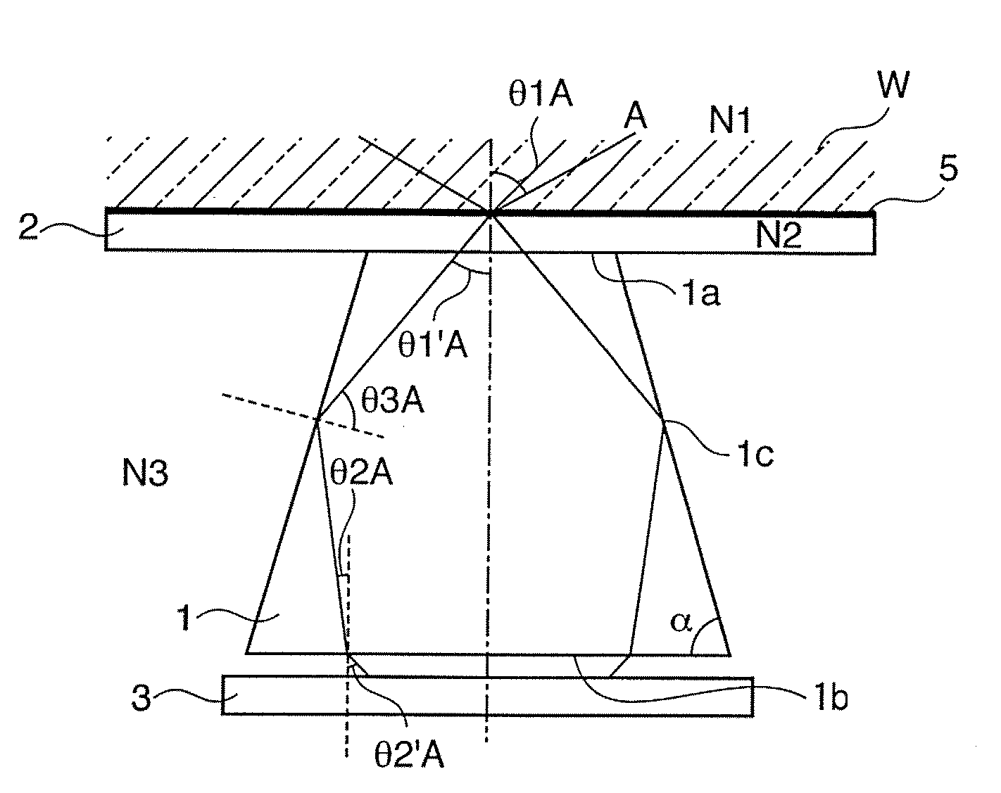
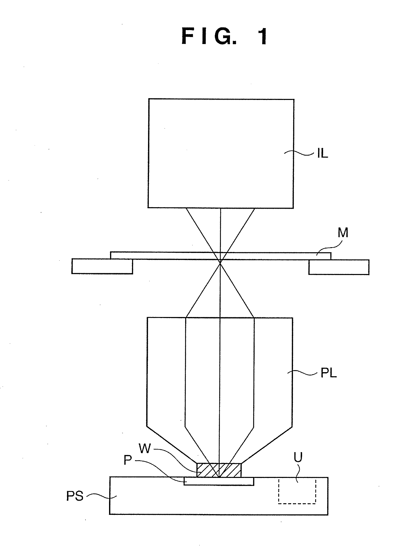
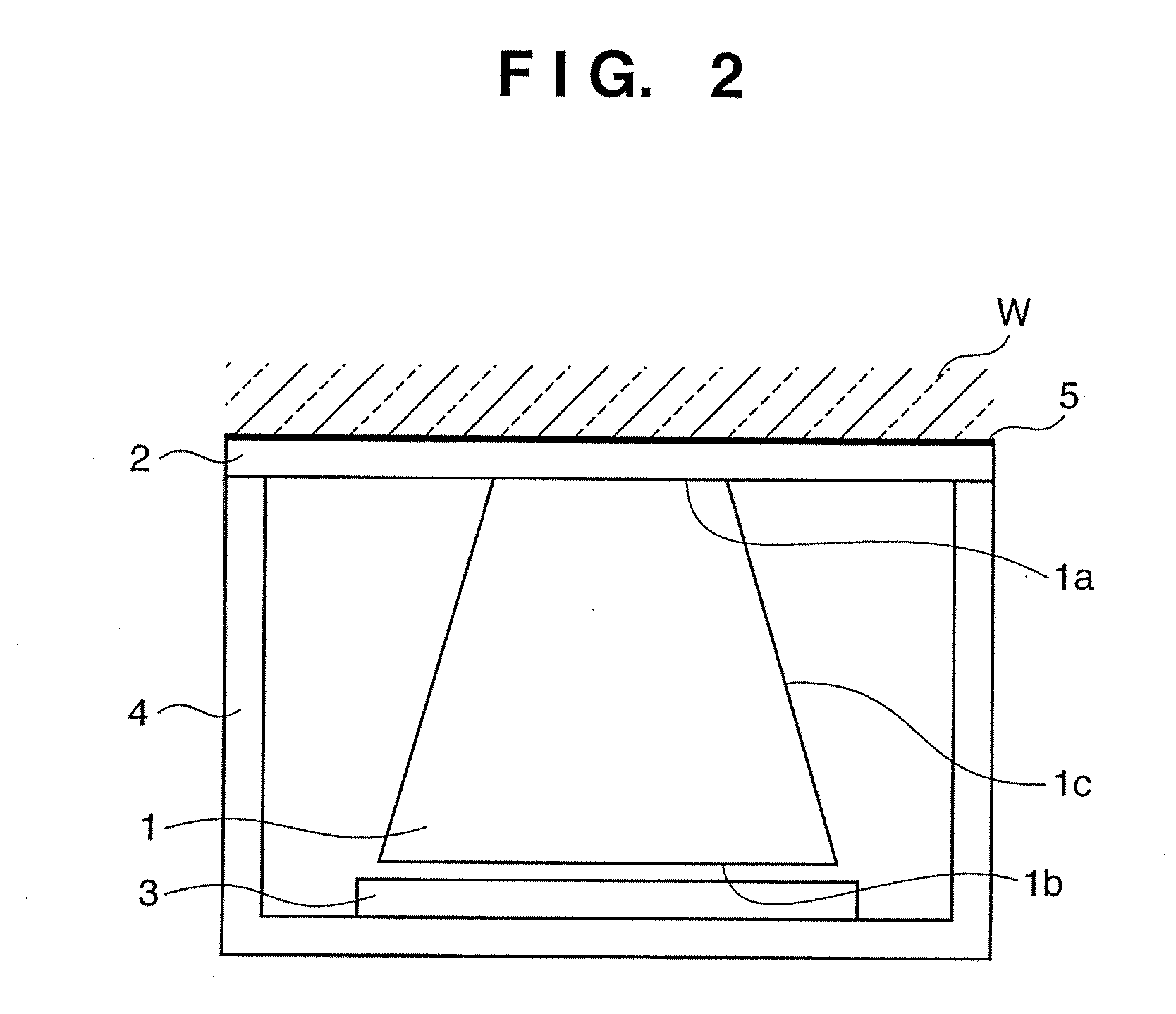
[0027]FIG. 1 is a schematic view showing an embodiment using an immersion exposure apparatus. The immersion exposure apparatus according to this embodiment includes an illumination optical system IL for guiding a light beam emitted by a light source to a mask (original) M, and a projection optical system PL for projecting the pattern image of the mask M onto a substrate P coated with a photosensitive material. The immersion exposure apparatus according to this embodiment achieves an increase in NA by filling the space between the lower end surface of the projection optical system PL and the surface of the substrate P with a liquid (immersion material) W and performing exposure. A light quantity sensor U is accommodated in a substrate stage PS to be flush with the substrate P. The light quantity sensor U is a sensor for detecting the light emerging from the proje...


PUM

PropertyMeasurementUnit
angleaaaaaaaaaa
refractive indexaaaaaaaaaa
incident angleaaaaaaaaaa

Abstract

An exposure apparatus comprising a projection optical system configured to project a pattern image of an original onto a substrate, and a sensor configured to detect light emerging from the projection optical system, the sensor including a light receiving element having a light receiving surface, and an optical member having a reflection surface which reflects the light emerging from the projection optical system toward the light receiving surface, wherein the reflection surface forms an acute angle with respect to the light receiving surface.

Description

BACKGROUND OF THE INVENTION[0001]1. Field of the Invention[0002]The present invention relates to an exposure apparatus and a device fabrication method.[0003]2. Description of the Related Art[0004]An exposure apparatus which projects and transfers a circuit pattern formed on a mask (reticle) onto a substrate such as a wafer via a projection optical system has conventionally been employed to fabricate a fine semiconductor device or a liquid crystal display device such as a semiconductor memory or logic circuit. The minimum dimension (resolution) of a pattern which can be transferred by the exposure apparatus is proportional to the exposure light wavelength, while it is inversely proportional to the numerical aperture (NA) of the projection optical system. In view of this, the shorter the wavelength and the higher the NA, the better the resolution. Along with the recent demand for micropatterning semiconductor devices, higher resolutions are becoming necessary.[0005]Immersion exposure ...

Claims


Application Information

Patent Timeline
Patent Type & Authority Applications(United States)
IPC IPC(8): G01N21/55G03F7/20H01L21/027
CPCG01N21/552G03F7/7085G03F7/70558G03F7/70341G03F7/2041G03F7/70233
Inventor SAITO, NOBUYUKIKAWASHIMA, HARUNA
Owner CANON KK
Why Eureka
Try Eureka