Surface foreign matter inspecting device

Inactive Publication Date: 2006-05-16
PANASONIC CORP
View PDF11 Cites 2 Cited by
  • Summary
  • Abstract
  • Description
  • Claims
  • Application Information

AI Technical Summary

Benefits of technology

[0010]With this configuration, the NA of the optical system can be enlarged with a simple configuration, the object point range on the object under inspection over which the detection optical system can capture the reflected light is broadened. The scanning range of the radiation optical system on the object under inspection is enlarged.

Problems solved by technology

Reductions of manufacturing yield in the manufacturing process of semiconductor devices have a direct effect in increasing the product's costs, so that the improvement of manufacturing yield has become an important challenge.
If the detection optical system 12 composed of ordinary optical elements as shown in FIG. 9 is used, then increasing the NA (numerical aperture) of the optical system in order to improve its focusing ability leads to the problem that the size of the detection optical system 12 becomes large, resulting in interference with light irradiated from the radiation optical system 5.
However, with

Method used


Image

  • Surface foreign matter inspecting device
  • Surface foreign matter inspecting device
  • Surface foreign matter inspecting device

Examples


Example

Embodiment 1

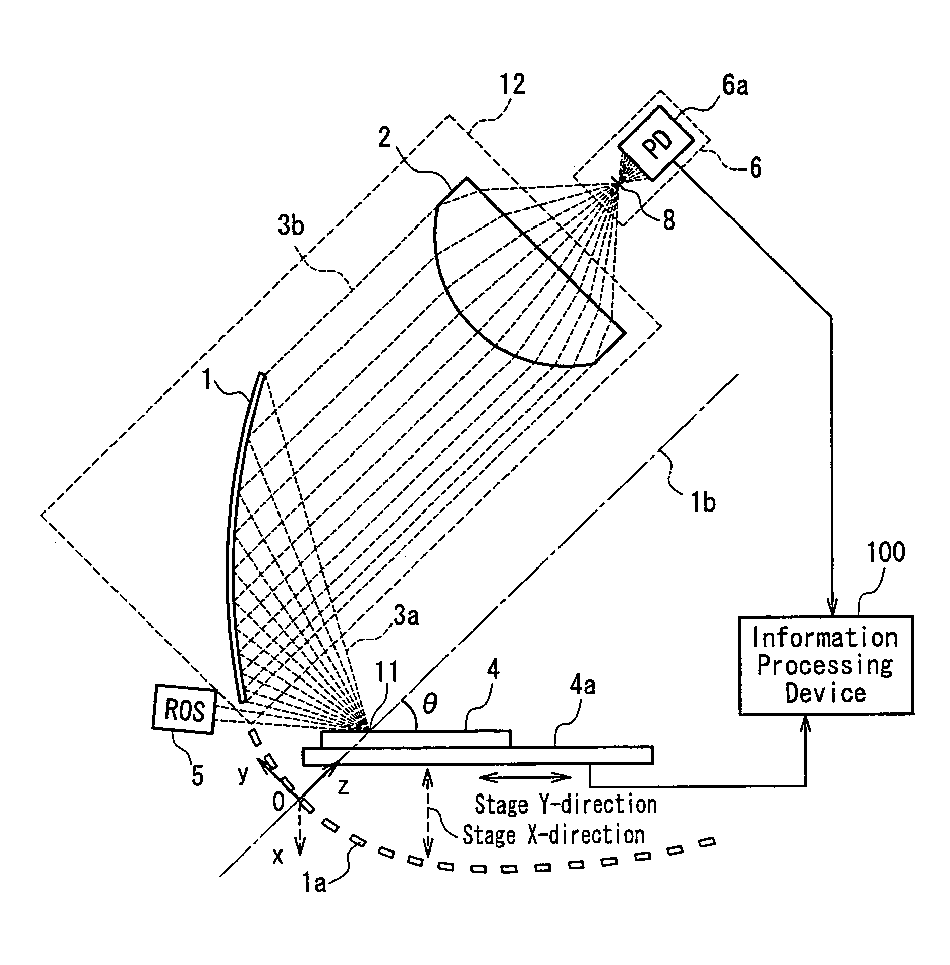
[0022]FIG. 1 is a schematic diagram showing a configuration of a surface foreign matter inspection device according to Embodiment 1 of the present invention. The configuration of this device is similar to that of the conventional surface foreign matter inspection device explained with reference to FIG. 9, except that the detection optical system 12 (focusing means) is configured by a cylindrical mirror 1 (first cylindrical mirror), which has a columnar surface or a substantially columnar surface, and a condensing lens 2 (condensing means), which has a rotation-symmetric shape. Consequently, portions having the same configuration and function as in the conventional example are given the same numerals, and their further explanation has been omitted.

[0023]In FIG. 1, numeral 1a denotes an extension surface (virtual surface) of the cylindrical mirror 1, numeral 1b denotes the optical axis of the cylindrical mirror 1, and numeral 11 denotes the irradiation position of the radi...

Example

Embodiment 2

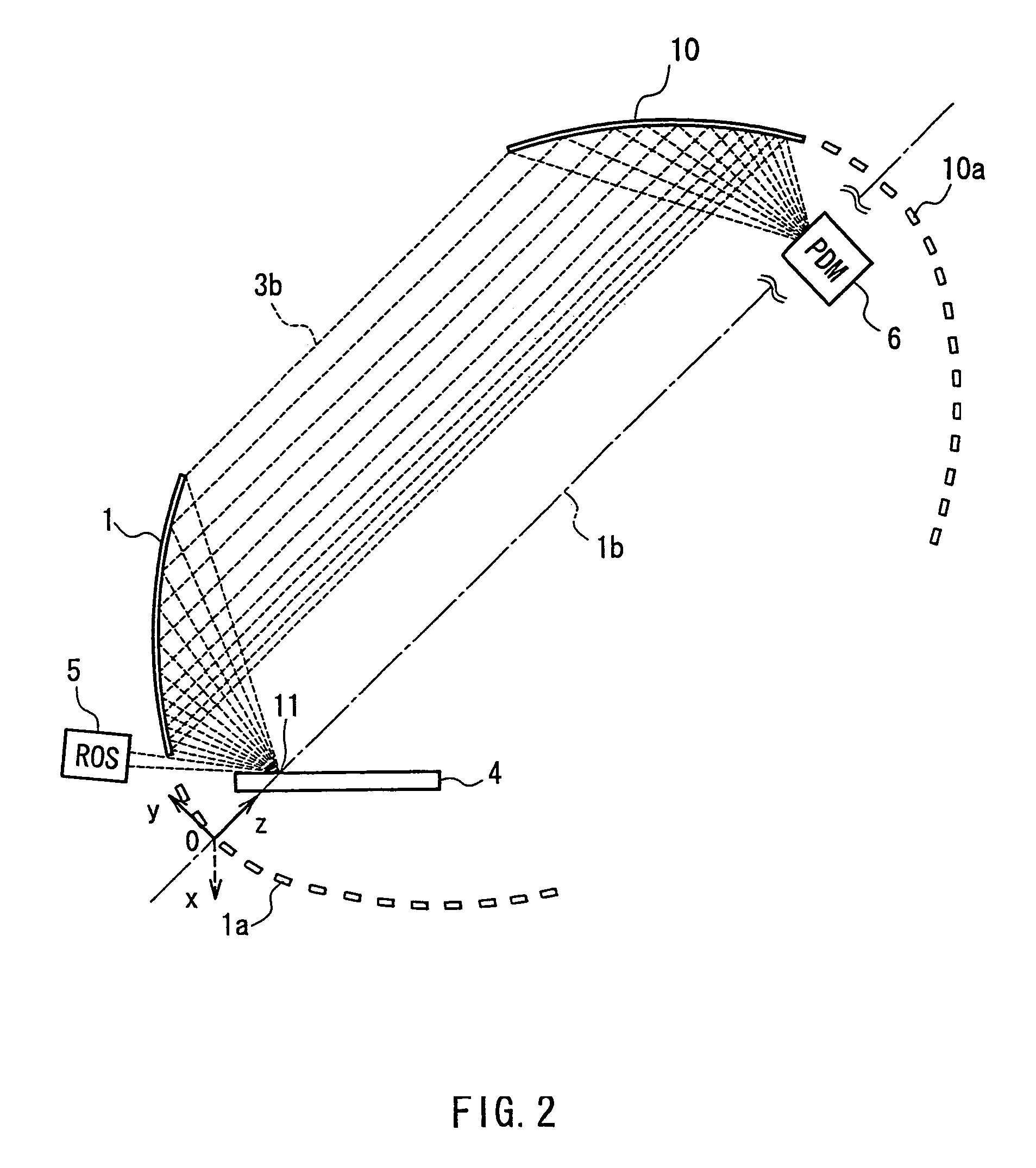
[0047]FIG. 2 is a schematic diagram showing a configuration of a surface foreign matter inspection device according to an embodiment of the present invention. The configuration of this device is similar to that of the device in Embodiment 1 (FIG. 1), except that in the detection optical system 12 of Embodiment 1, a cylindrical mirror 10 (second cylindrical mirror serving as light condensing means) whose optical axis substantially coincides with that of the cylindrical mirror 1 (first cylindrical mirror) is used instead of the condensing lens 2. In FIG. 2, numeral 10a denotes the extension surface (virtual surface) of the cylindrical mirror 10. Other portions corresponding to FIG. 1 have been given the same numerals, and their further explanation has been omitted. The coordinate system is the same as in FIG. 1.

[0048]Using this embodiment, foreign matter on the silicon wafer 4 can be inspected as follows. As in Embodiment 1, irradiation light is irradiated onto the foreign...

Example

Embodiment 3

[0053]FIG. 3 is a schematic diagram showing a configuration of a surface foreign matter inspection device according to Embodiment 3 of the present invention. The configuration of this device is similar to that of the device in Embodiment 1 (FIG. 1), except that in the detection optical system 12 of Embodiment 1, a cylindrical lens 2a having a lens effect in the x-axis direction is disposed between the cylindrical mirror 1 and the condensing lens 2. Other portions corresponding to FIG. 1 have been given the same numerals, and their further explanation has been omitted. Also the coordinate system is the same as in FIG. 1. It should be noted that in FIG. 3, numeral 15 denotes a cross-sectional view taken along the zx-plane of the cylindrical lens 2a and the condensing lens 2 (in the following embodiments, the corresponding portions of the referenced drawings are the same).

[0054]Using this device, foreign matter on the silicon wafer 4 can be inspected as follows. As in Embod...


PUM


Abstract

A surface foreign matter inspection device is provided with which the NA can be enlarged with a simple configuration, and a shortening of the time required for foreign matter inspection as well as a high detection sensitivity can be achieved. The device is provided with an optical detection means 6 that irradiates light from an radiation optical system onto the surface of an object under inspection on a stage, reflects light scattered by foreign matter on the object under inspection and turns the reflected light into parallel light, condenses the parallel light with a condensing lens, and detects the condensed light, as well as an information processing device 100 for processing an electrical signal from the optical detection means 6 and position information regarding the foreign matter on the object under inspection 4.

Description

TECHNICAL FIELD[0001]The present invention relates to surface foreign matter inspection devices that detect the state of foreign matter adhering to the surface of a semiconductor substrate.BACKGROUND ART[0002]Reductions of manufacturing yield in the manufacturing process of semiconductor devices have a direct effect in increasing the product's costs, so that the improvement of manufacturing yield has become an important challenge. One of the main factors leading to a decrease in manufacturing yield is the adherence of foreign matter to the semiconductor substrate, so that there is a strong demand for a technology for detecting the state of adherence of foreign matter efficiently and with high sensitivity.[0003]Conventionally, it is well known to use optical means as a technology for detecting foreign matter on a semiconductor substrate. FIG. 9 is a schematic diagram showing a configuration example of a conventional surface foreign matter inspection device using optical means. In FIG...

Claims


Application Information

Patent Timeline
IPC IPC(8): G01N21/00G01N21/88G01N21/956G01N21/94G01N21/95H01L21/66
CPCG01N21/8806G01N21/9501G01N21/94
Inventor KIMURA, SYUNSUKEYAMAMOTO, YOSHIHARU
Owner PANASONIC CORP
Why Eureka
Try Eureka