
Exposure apparatus, exposure method, and device fabrication method

a technology of exposure apparatus and fabrication method, which is applied in the direction of optical radiation measurement, printers, instruments, etc., can solve the problems of incident light distorted irrespective of whether, light at an off-axis position along the optical axis (the center of curvature) is distorted, and the above-described sensor cannot receive full-aperture light, etc., to achieve the effect of increasing the na and high precision

Inactive Publication Date: 2011-09-06
CANON KK
View PDF6 Cites 1 Cited by
  • Summary
  • Abstract
  • Description
  • Claims
  • Application Information

AI Technical Summary

Benefits of technology

[0012]The present invention provides an exposure apparatus which is advantageous to increasing the NA by, for example, immersion exposure and can measure an optical characteristic with high precision.

Problems solved by technology

For this reason, the above-described sensors often cannot receive full-aperture light.
Unfortunately, when the exit side of a measurement substrate is curved or a planoconvex lens with a curvature is arranged in contact with or adjacent to a measurement substrate, light at an off-axis position along the optical axis (the center of curvature) is distorted due to the curvature, although that at an on-axis position is free from any such influence.
If the measurement substrate suffers a manufacturing error such as a drawing error generated upon drawing a transmission part or a positioning error of a planoconvex lens to be arranged in contact with or adjacent to the measurement substrate, incident light is distorted irrespective of whether it is on- or off-axis.
Upon receiving light distorted due to such factors, the sensors output optical characteristic measurement results with errors (measurement errors), resulting in significant decreases in measurement precision.
If a plurality of transmission parts is formed on a measurement substrate, regions where these transmission parts can be formed are limited under the influence of light distortion.

Method used


Image

  • Exposure apparatus, exposure method, and device fabrication method
  • Exposure apparatus, exposure method, and device fabrication method
  • Exposure apparatus, exposure method, and device fabrication method

Examples


Embodiment Construction

[0032]A preferred embodiment of the present invention will be described below with reference to the accompanying drawings. The same reference numerals denote the same members throughout the drawings, and a repetitive description thereof will not be given.

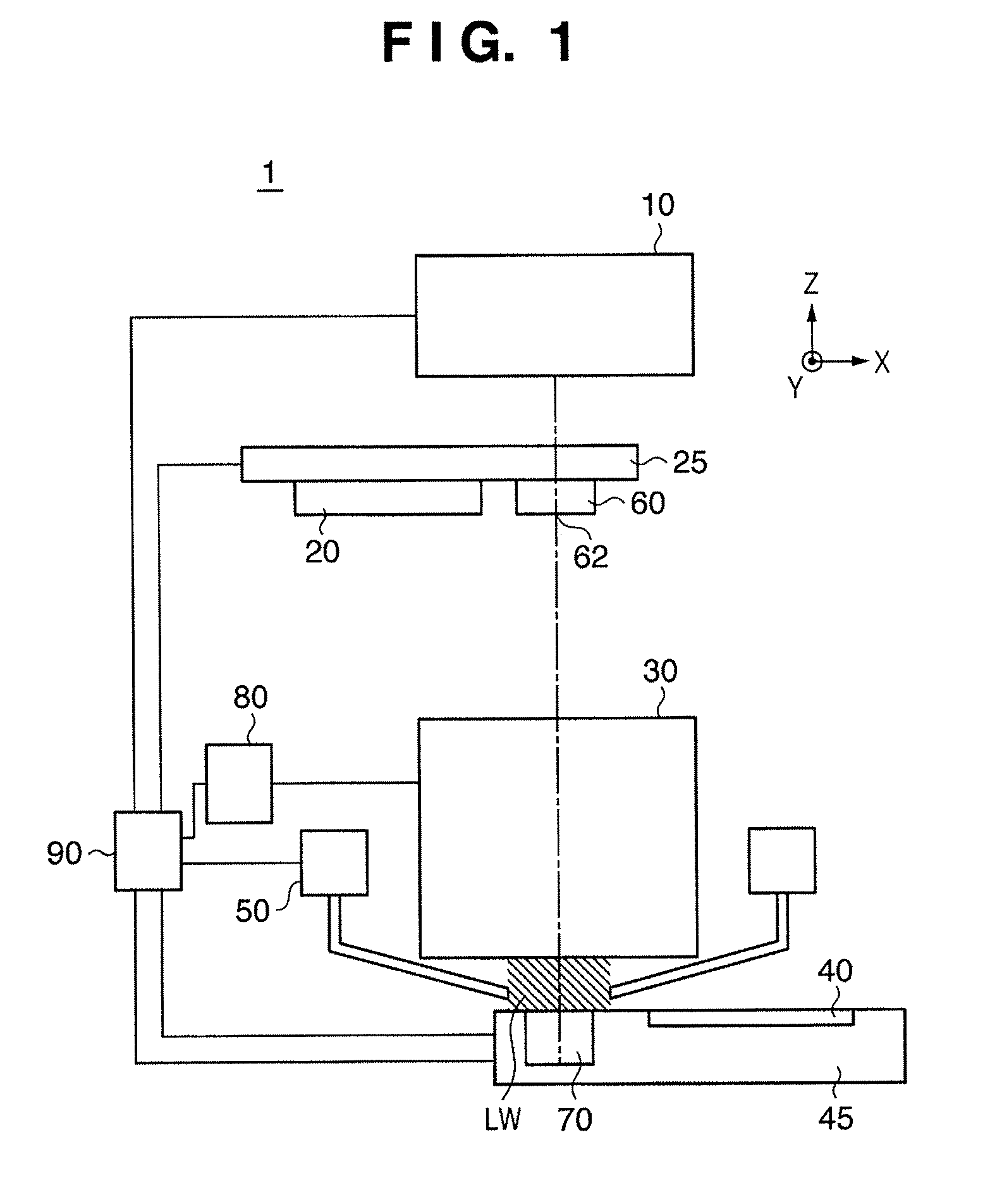
[0033]FIG. 1 is a schematic sectional view showing the arrangement of an exposure apparatus 1 according to one aspect of the present invention. The exposure apparatus 1 is an immersion exposure apparatus which transfers the pattern of a reticle 20 onto a wafer 40 by exposure using the step & scan scheme via a liquid LW supplied between a projection optical system 30 and the wafer 40. However, the exposure apparatus 1 can also adopt the step & repeat scheme. As shown in FIG. 1, the exposure apparatus 1 includes an illumination apparatus 10, a reticle stage 25, the projection optical system 30, a wafer stage 45, a liquid supply-recovery mechanism 50, a reticle side reference plate 60, a light-receiving device 70, an adjuster 80, and a...


PUM


Abstract

The present invention provides an exposure apparatus which exposes a substrate via a liquid, comprising a measurement substrate including a transmission part configured to transmit a light beam having passed through a projection optical system, a light-receiving unit including a light-receiving surface configured to receive the light beam transmitted through the liquid and the transmission part, and a calculator configured to arithmetically convert a light intensity distribution, on the light-receiving surface, of the light beam received by the light-receiving surface into a light intensity distribution on a pupil plane of the projection optigottacal system, based on information indicating a correlation between a position coordinate on the light-receiving surface and a position coordinate on the pupil of the projection optical system.

Description

BACKGROUND OF THE INVENTION[0001]1. Field of the Invention[0002]The present invention relates to an exposure apparatus, an exposure method, and a device fabrication method.[0003]2. Description of the Related Art[0004]A projection exposure apparatus has conventionally been employed to fabricate, for example, a micropatterned semiconductor device such as a semiconductor memory or logic circuit by using photolithography. The projection exposure apparatus transfers a circuit pattern formed on a reticle (mask) onto, for example, a wafer via a projection optical system.[0005]A minimum dimension (resolution) that a projection exposure apparatus can transfer is proportional to the wavelength of exposure light and is inversely proportional to the numerical aperture (NA) of a projection optical system. The shorter the wavelength and the higher the NA, the better the resolution. Along with the recent demand for micropatterning semiconductor devices, the wavelength of exposure light is shorteni...

Claims


Application Information

Patent Timeline
Patent Type & Authority Patents(United States)
IPC IPC(8): G03B27/68
CPCG03F7/70258G03F7/70341G03F7/70508G03F7/70666G03F7/7085
Inventor MIYAHARU, TAKAFUMI
Owner CANON KK
Learn More