Composite thermal interface material system and method using nano-scale components

a thermal interface and nano-scale technology, applied in the field of thermal interface materials (tims), can solve the problems of significant thermal resistance, difficult to meet the needs of nano-scale components, so as to reduce mechanical stress, reduce stress, and reduce the effect of mechanical stress

Active Publication Date: 2009-10-29
THE RES FOUND OF STATE UNIV OF NEW YORK
View PDF9 Cites 36 Cited by
  • Summary
  • Abstract
  • Description
  • Claims
  • Application Information

AI Technical Summary

Benefits of technology

[0023]It is especially desirable to manufacture a material in accordance with a method that includes stabilizing nano-scale fibers—prior to applying them to a device requiring a TIM—with a stabilizing material to create a stabilized fiber assembly. The stabilizing material may be a filler disposed amongst the nano-scale fibers. The stabilizing material may be a capping layer added to the fibers. There may be both stabilizing material and at least one capping layer. There may be two capping layers, creating a sandwich-like composite system. Each capping layer may be made of two (or more) sub-layers. Advantageously, the capping material may be a nano- or micro-particle paste that achieves the goals above of attaching the TIM, aligning the nano-scale fibers, and improving thermal conduction. The particles, in turn may be isotropic or anisotropic, and in the case of anisotropic particles, may be anisotropically aligned. Advantageously, the paste may be located adjacent to thermal hotspots in the material to be cooled, while voids in the paste, to improve processing, may be selectively located adjacent spots not expected to get so hot. Thus, for example, voids in the TIM may be statistically difficult to avoid, but may be selectively disposed in areas where they are tolerated. In some cases, a void may be desired, for example to help maintain a spatially uniform device temperature in spite of regionally varying heat dissipation.
[0042]The thermal interface material may be adapted to reduce mechanical stresses that arise between devices coupled by the thermal interface material as compared to a direct bonding of surfaces of the devices. The thermal interface material may also be adapted to reduce a stress between devices cause by at least one of differences in coefficient of thermal expansion, or differences in temperature.
[0043]The material as provided may comprise areas having low modulus of elasticity, whereby stresses in an assembly composed of a device, a heat sink, and the thermal interface material disposed between respective surfaces of the device and the heat sink, are reduced.

Problems solved by technology

Challenges in designing a thermal interface material arise due to interfacial resistances, which are a function of surface conditions (devices and heat-sinks or heat spreaders), material properties of the TIM, and the assembly processes used to deposit the TIM and get it to the design point thickness.
The interfaces are particularly problematic since they represent a transition between different materials and may contain air voids and other defects.
Interfaces typically result in significant thermal resistances.
This method tends to be cost-prohibitive.
Thermal interface materials are particularly vulnerable to damage under some application conditions because they may interface between materials with significantly different thermo mechanical properties such as coefficient of thermal expansion and modulus of elasticity.
In many applications, such cycles occur for thousands of times during the life of the product.
Another issue to be addressed is the impact of the thermal interface material on overall system cost.
While the cost of the interface material may be small, if it requires special assembly or handling processes that may slow down the overall assembly process then that may significantly impact the overall system cost.

Method used


Image

  • Composite thermal interface material system and method using nano-scale components
  • Composite thermal interface material system and method using nano-scale components
  • Composite thermal interface material system and method using nano-scale components

Examples


Embodiment Construction

[0069]For the purposes of this application the terms “nanometer realm” or “nano-scale” are understood to mean approximately 1-100 nm, and preferably 1-10 nm. “Nano-particles” will be in this same size range. Micro range will be understood to mean 0.1 to about 10 microns.

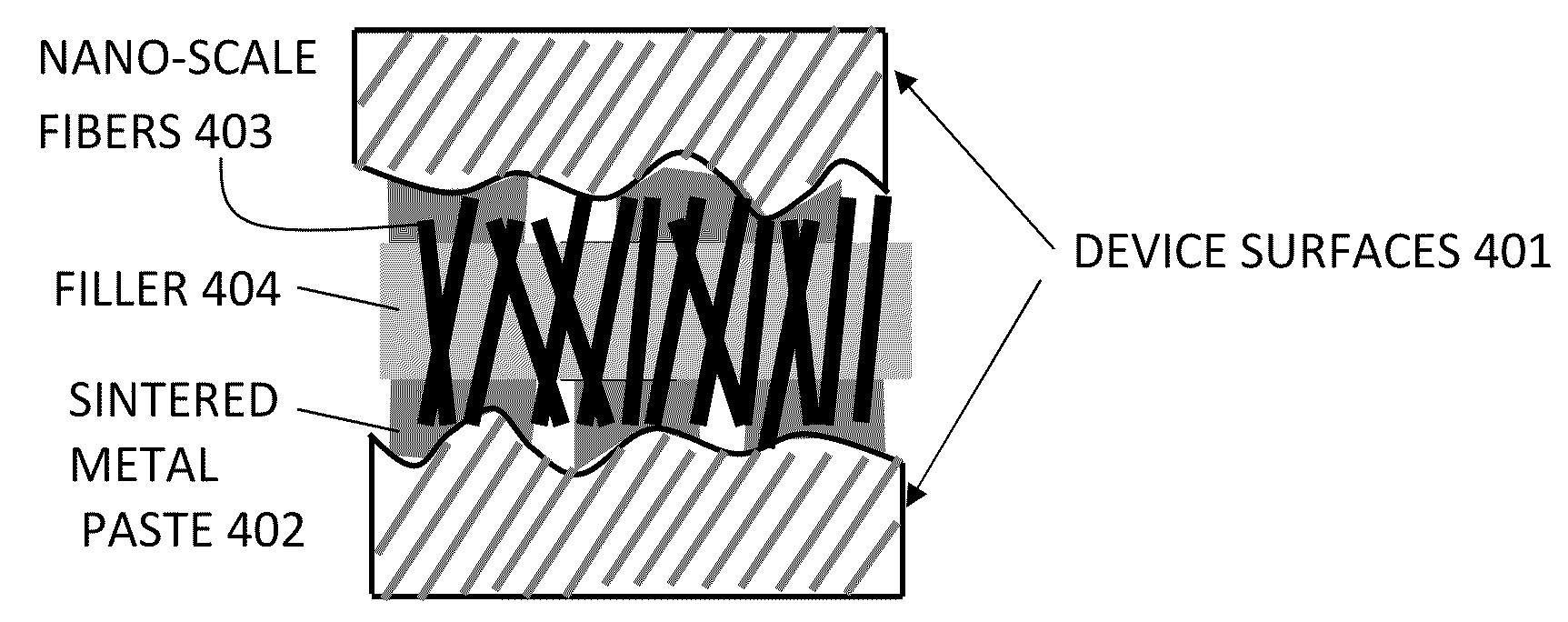
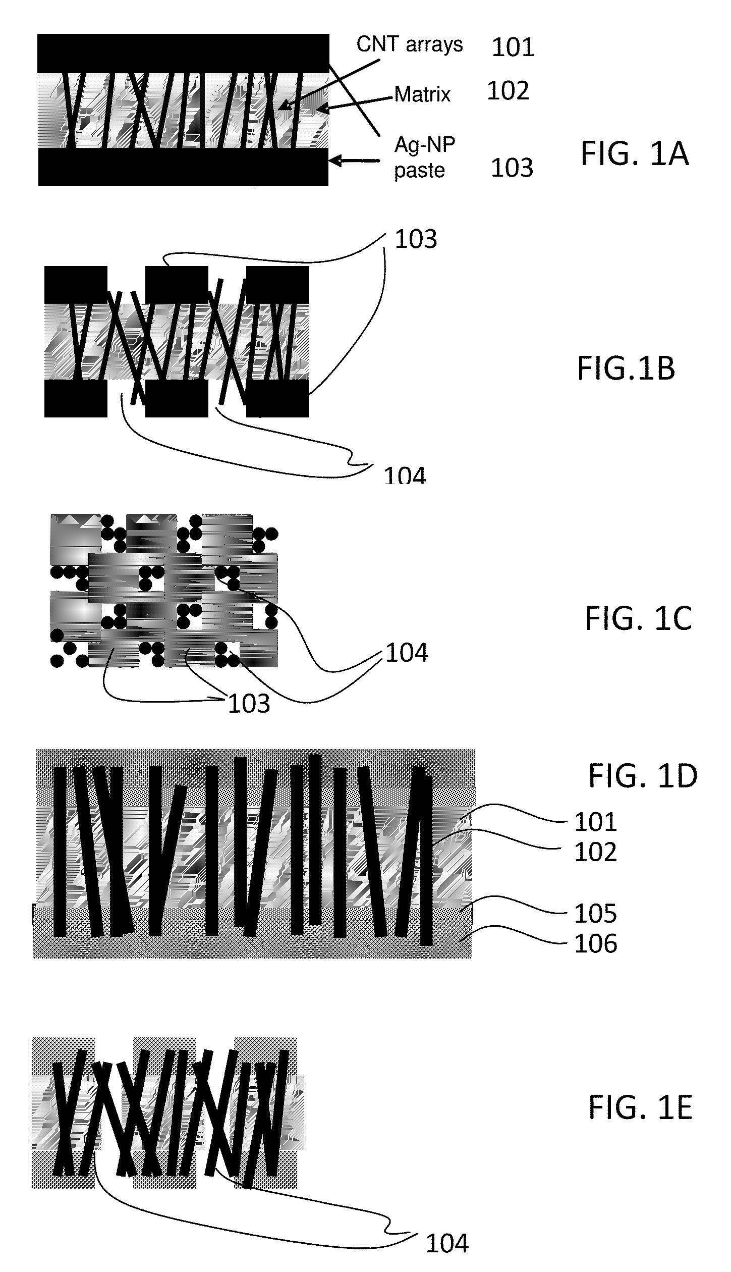
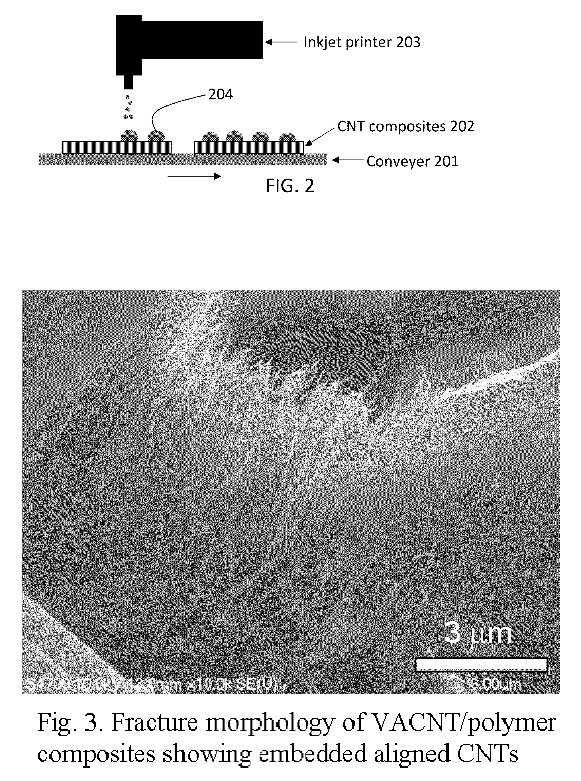
[0070]FIG. 1A is a schematic diagram of a TIM system in accordance with the invention. FIG. 1A illustrates nano-scale fibers 101, such as CNT's stabilized in a matrix 102 and sandwiched between two capping layers 103, such as silver nanoparticle paste. The fibers 101 may be vertically aligned or randomly oriented. There will be some expense associated with getting the fibers to be aligned, but aligned fibers are expected to demonstrate superior performance, and are therefore preferred. On the other hand, even in an unaligned state, a portion of the fibers 101 will be oriented normal to the interface plane. The matrix 102 may include organic or organic / inorganic hybrid material stabilizing the arrays or networks of na...


PUM

PropertyMeasurementUnit
sizeaaaaaaaaaa
temperatureaaaaaaaaaa
heightaaaaaaaaaa

Abstract

A method of manufacturing a thermal interface material, comprising providing a sheet comprising nano-scale fibers, the sheet having at least one exposed surface; and stabilizing the fibers with a stabilizing material disposed in at least a portion of a void space between the fibers in the sheet. The fibers may be CNT's or metallic nano-wires. Stabilizing may include infiltrating the fibers with a polymerizable material. The polymerizable material may be mixed with nano- or micro-particles. The composite system may include two films, with the fibers in between, to create a sandwich. Each capping film may include two sub films: a palladium film closer to the stabilizing material to improve adhesion; and a nano-particle film for contact with a device to be cooled or a heat sink.

Description

RELATED APPLICATION[0001]The present application claims benefit of priority from U.S. Provisional Patent Application No. 61 / 037,125, filed Mar. 17, 2008, and from U.S. Provisional Patent Application No. 61 / 037,132, filed Mar. 17, 2008, each of which is expressly incorporated herein by reference in its entirety.BACKGROUND OF THE INVENTION[0002]1. Field of the Invention[0003]The invention relates to the field of thermal interface materials (TIMs) for use in electronic devices or other thermal management applications that require rapid dissipation of heat. Examples of devices needing TIMs include computers, telecommunications, space, military, and medical apparatus.[0004]2. Related Art[0005]Power dissipation in electronic devices is projected to increase significantly over the next ten years to the range of 100-150 Watts per cm2 for high performance applications1. This increase in power represents a major challenge to systems integration since the maximum device temperature needs to be...

Claims


Application Information

Patent Timeline
Patent Type & Authority Applications(United States)
IPC IPC(8): B32B15/01B32B15/08B32B5/16C09K5/00
CPCH01L23/373H01L23/433H01L2224/16H01L2224/73253H01L2924/01012H01L2924/0102Y10T428/25H01L2924/01078H01L2924/16195H01L2924/01019Y10S977/742Y10T428/12007H01L2924/01046Y10S977/762Y10T428/31678
Inventor WANG, HAOSAMMAKIA, BAHGATLIU, YAYONGYANG, KAIKUN
Owner THE RES FOUND OF STATE UNIV OF NEW YORK
Why Eureka
Try Eureka