Apparatus for producing electron source

a technology for producing electron sources and manufacturing apparatuses, applied in the manufacture of electrode systems, electrode system manufacturing, tube/lamp factory adjustment, etc., can solve the problem of requiring a long time for second manufacturing methods, and achieve the effect of convenient downsizing and operation

Inactive Publication Date: 2004-04-27
CANON KK
View PDF16 Cites 54 Cited by
  • Summary
  • Abstract
  • Description
  • Claims
  • Application Information

AI Technical Summary

Benefits of technology

It is an object of the present invention to provide an electron source manufacturing apparatus which can be easily downsized and operated.

Problems solved by technology

However, the first manufacturing method requires a larger vacuum chamber and an exhaust device coping with a high vacuum as the size of the electron source substrate increases.
The second manufacturing method requires a long time for evacuation from the inner space of the panel of the image forming apparatus and introduction of gas containing an organic substrate into the inner space of the panel.

Method used


Image

  • Apparatus for producing electron source
  • Apparatus for producing electron source
  • Apparatus for producing electron source

Examples


example 1

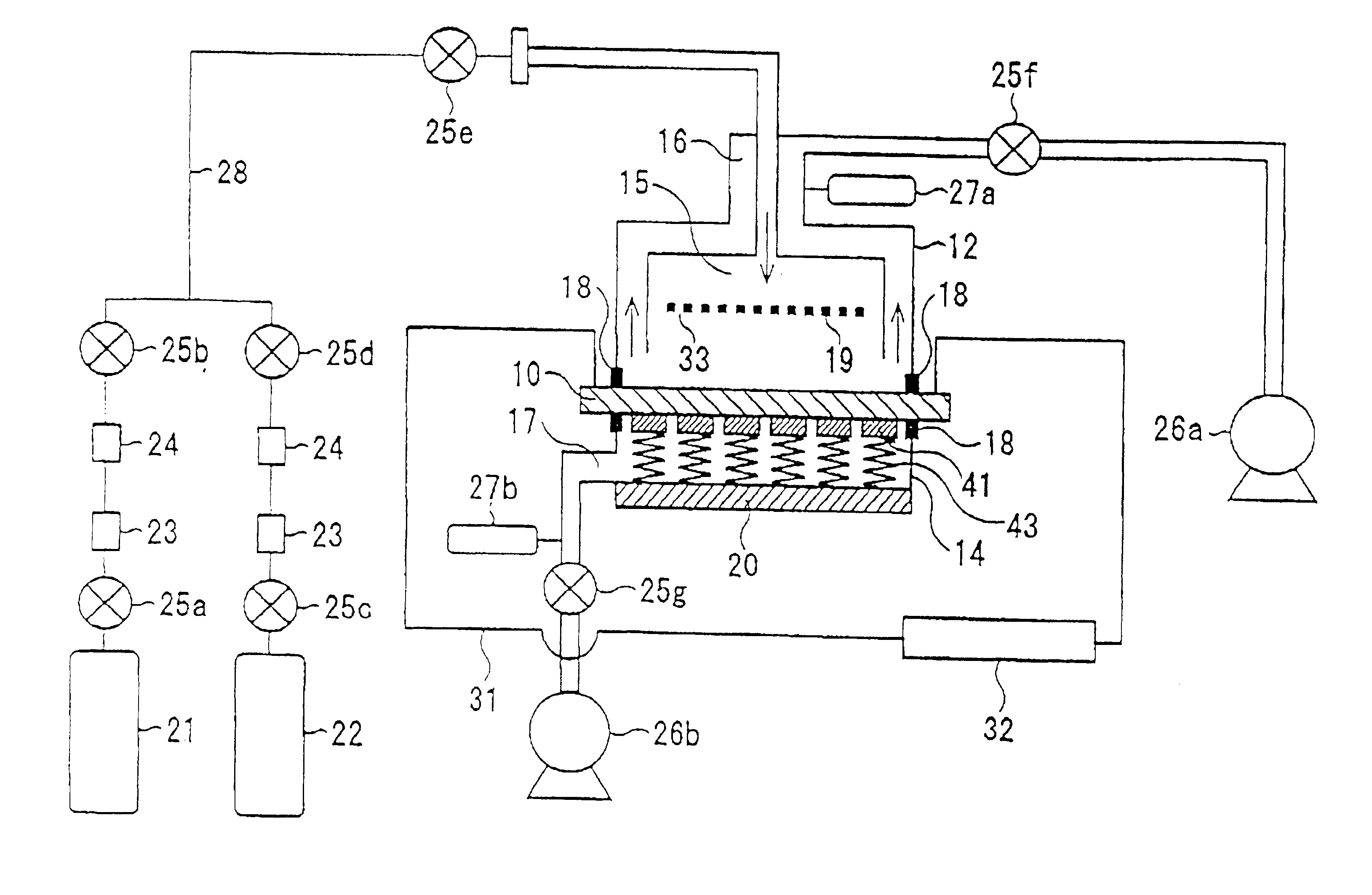
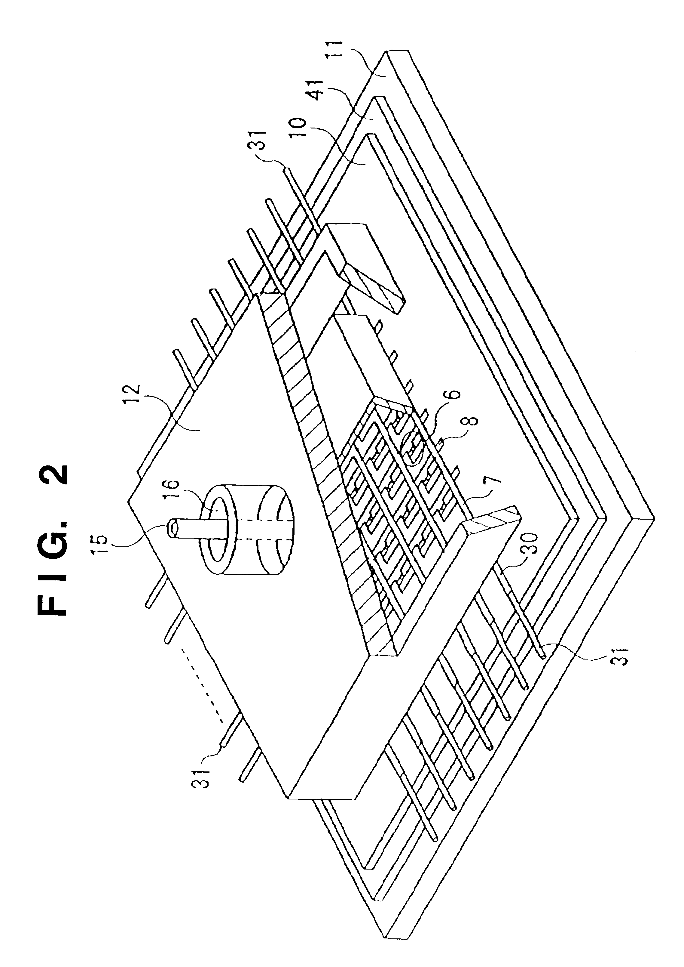
This example manufactures an electron source shown in FIG. 24 having a plurality of surface-conduction type electron-emitting devices shown in FIGS. 22 and 23 by using the manufacturing apparatus according to the present invention. In FIGS. 22 to 24, reference numeral 101 denotes a substrate; 2 and 3, device electrodes; 4, a conductive film; 29, a carbon film; and 5, a gap in the carbon films 29. Reference symbol G denotes a gap G in the conductive film 4. Pt paste was printed by an offset printing method on a glass substrate (350.times.300 mm in size and 5 mm in thickness) having an SiO.sub.2 layer, and heated and baked to form device electrodes 2 and 3 shown in FIG. 25 with a thickness of 50 nm. Ag paste was printed by a screen printing method, and heated and baked to form X-direction wiring lines 7 (240 lines) and Y-direction wiring lines 8 (720 lines) shown in FIG. 25. At the intersections of the X-direction wiring lines 7 and Y-direction wiring lines 8, insulating pastes were p...

example 2

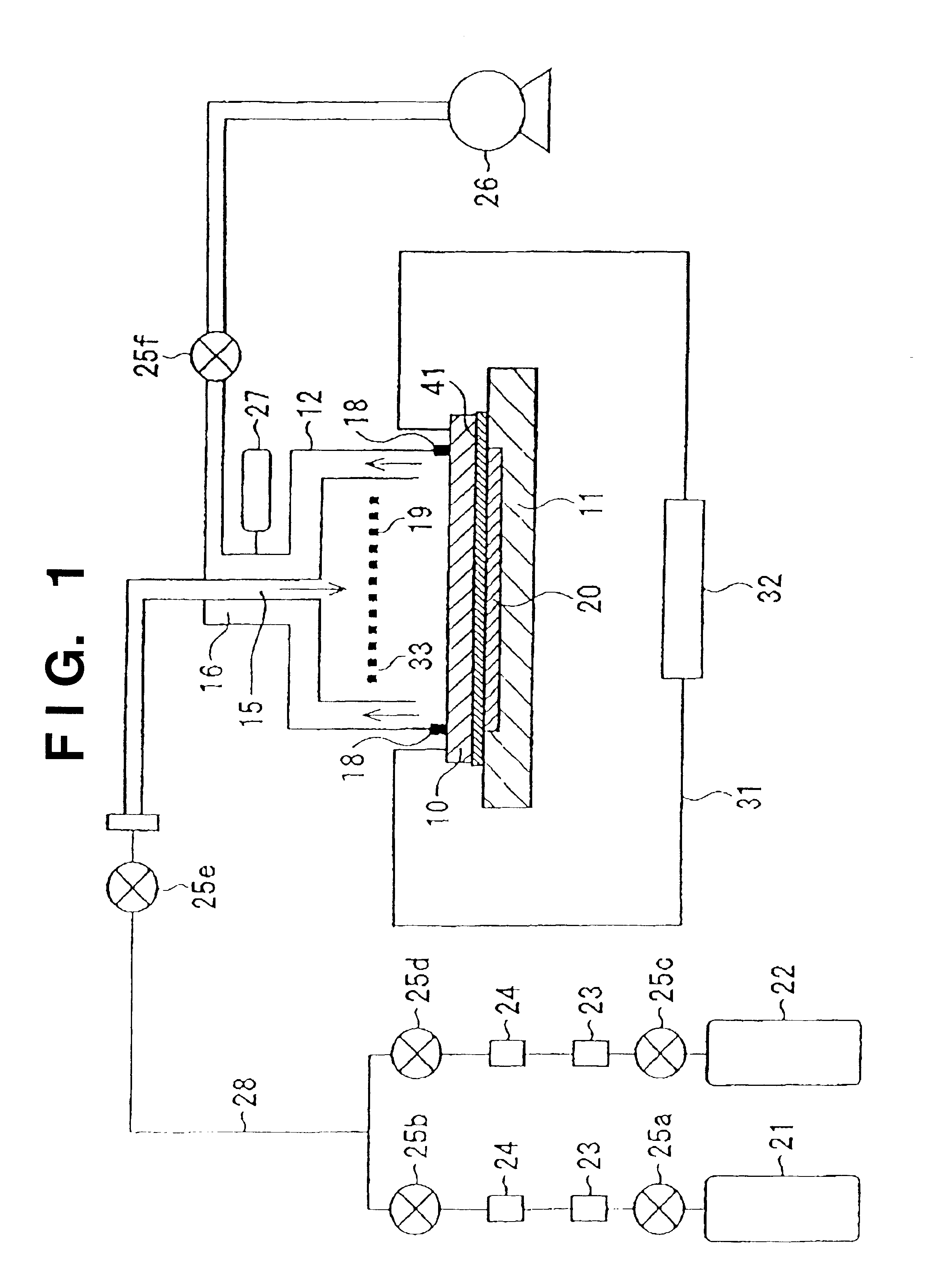
An electron source substrate 10 shown in FIG. 25 that was identical to the substrate 10 in Example 1 was fabricated and set in the manufacturing apparatus of FIG. 1. In this example, a gas mixture containing an organic substance was heated to 80.degree. C. by a heater arranged around a pipe 28, and then introduced into a vacuum vessel 12. The electron source substrate 10 was heated via a heat conduction member 41 using a heater 20 inside a support 11 to set the substrate temperature to 80.degree. C. Except for this, activation processing was executed similarly to Example 1, thereby fabricating an electron source.

Carbon films 29 were formed via a gap 5 on an electron-emitting device having undergone activation processing, as shown in FIGS. 23 and 24.

Similar to Example 1, this example could perform activation processing within a short time. The device current If at the end of activation processing was measured similarly to Example 1 to find that the device current If increased about 1...

example 3

An electron source was fabricated by the same method as in Example 1 except that the manufacturing apparatus shown in FIG. 3 was used for an electron source substrate 10 shown in FIG. 25 that was identical to the substrate 10 in Example 1, and silicone oil was used as a heat conduction member.

In the apparatus of this example, holes (not shown) serving as both air holes and viscous liquid substance discharge holes were formed at positions on an almost diagonal line outside the device electrode region so as not to leave air between the lower surface of the substrate and a support in injecting silicone oil below the substrate using a viscous liquid substance inlet pipe. The device current value at the end of activation processing was the same as the result of Example 1.


PUM

PropertyMeasurementUnit
pressureaaaaaaaaaa
voltageaaaaaaaaaa
thicknessaaaaaaaaaa

Abstract

This invention provides an electron source manufacturing apparatus which can be easily downsized and operated. The electron source manufacturing apparatus includes a support member for supporting a substrate (10) having a conductor (11), a vessel (12) which has a gas inlet port (15) and a gas exhaust port (16) and covers a partial region of the surface of the substrate (10); a gas inlet unit (24) connected to the gas inlet port (15) to introduce gas into the vessel, an exhaust unit (26) connected to the gas exhaust port to evacuate the interior of the vessel, and a voltage application unit (32) for applying a voltage to the conductor.

Description

The present invention relates to an electron source manufacturing apparatus and manufacturing method.Conventionally, two types of devices, namely thermionic electron-emitting devices and cold cathode electron-emitting devices, are known as electron-emitting devices. The cold cathode electron-emitting devices include field emission type electron-emitting devices, metal / insulator / metal type electron-emitting devices, and surface-conduction type electron-emitting devices.The surface-conduction type electron-emitting device utilizes the phenomenon that electrons are emitted by flowing a current through a small-area thin film formed on a substrate, in parallel with the film surface. The present applicants have made many proposals for surface-conduction type electron-emitting devices having novel arrangements and their applications. The basic arrangement, manufacturing method, and the like are disclosed in, e.g., Japanese Patent Laid-Open Nos. 7-235255 and 8-171849.The surface-conduction ...

Claims


Application Information

Patent Timeline
Patent Type & Authority Patents(United States)
IPC IPC(8): H01J9/02
CPCH01J9/027H01J1/30
Inventor TAKEDA, TOSHIHIKOKAMIO, MASARUYAMASHITA, MASATAKASATO, YASUEODA, HITOSHIYAMAMOTO, KEISUKETAMURA, MIKIKAWASAKI, HIDESHIJINDAI, KAZUHIRO
Owner CANON KK
Why Eureka
Try Eureka