Method of manufacturing PCB and PCB manufactured by the same

a manufacturing method and technology of printed circuit boards, applied in the direction of printed circuit manufacturing, printed circuit aspects, printed element electric connection formation, etc., can solve the problems of inability to manufacture products in any other way, various functions, and the growth of the pcb market in korea is at a standstill, so as to enhance the reliability of products, prevent the formation of attachment defects of copper clad layers, and enhance the effect of product reliability

Inactive Publication Date: 2009-11-12
SAMSUNG ELECTRO MECHANICS CO LTD
View PDF0 Cites 18 Cited by
  • Summary
  • Abstract
  • Description
  • Claims
  • Application Information

AI Technical Summary

Benefits of technology

[0013]An advantage of the present invention is that it provides a method of manufacturing a PCB, in which a via hole is formed in a substrate including an aluminum core, the surface of an aluminum core corresponding to the inner surface of the via hole is substituted with a zinc film, the zinc film is substituted with a nickel film, and electroless plating and electroplating are sequentially formed on the via hole. Therefore, the aluminum core can be prevented from corroding during the electroless plating, and attachment defects of a copper clad layer can be prevented from occurring, which makes it possible to enhance the reliability of products.
[0014]Another advantage of the invention is that it provides a PCB manufactured by the method of manufacturing a PCB.
[0015]Additional aspects and advantages of the present general inventive concept will be set forth in part in the description which follows and, in part, will be obvious from the description, or may be learned by pra

Problems solved by technology

Currently, the growth of the PCB market in Korea is at a standstill.
These products cannot be manufactured in any other Asian countries than Korea, because a high-level technology should be required.
One of prominent features in the digital electronic appliances is that various functions are added thereto and power consumption thereof increases.
However, since the conventional PCB has a m

Method used


Image

  • Method of manufacturing PCB and PCB manufactured by the same
  • Method of manufacturing PCB and PCB manufactured by the same
  • Method of manufacturing PCB and PCB manufactured by the same

Examples


Embodiment Construction

[0036]Reference will now be made in detail to the embodiments of the present general inventive concept, examples of which are illustrated in the accompanying drawings, wherein like reference numerals refer to like elements throughout. The embodiments are described below in order to explain the present general inventive concept by referring to the figures.

[0037]Hereinafter, a method of manufacturing a PCB and a PCB manufactured by the same according to the present invention will be described in detail with reference to the accompanying drawings.

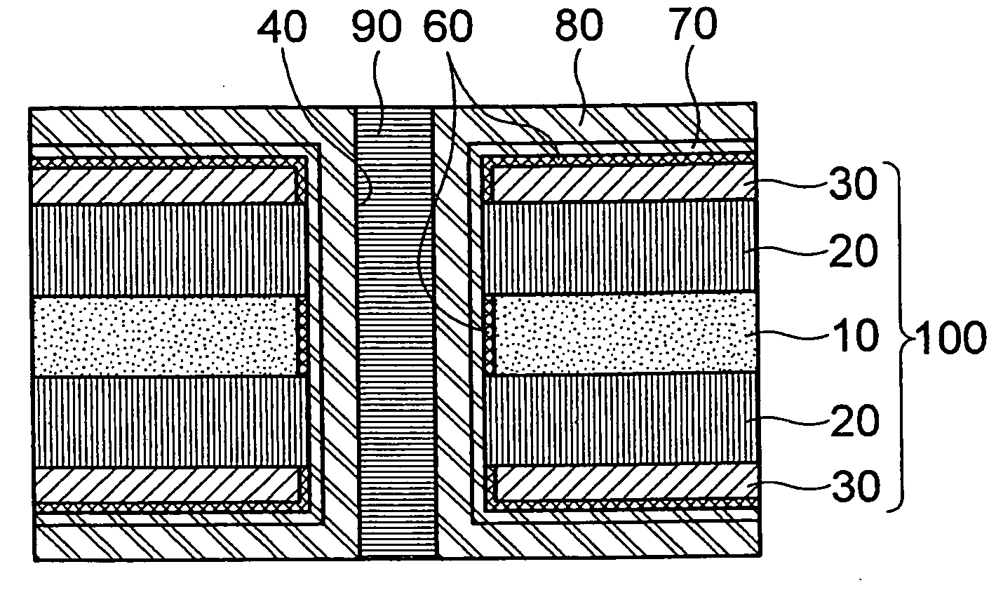
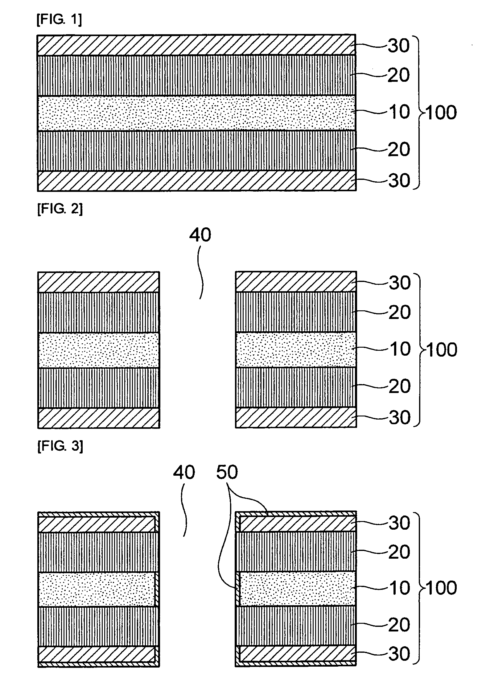
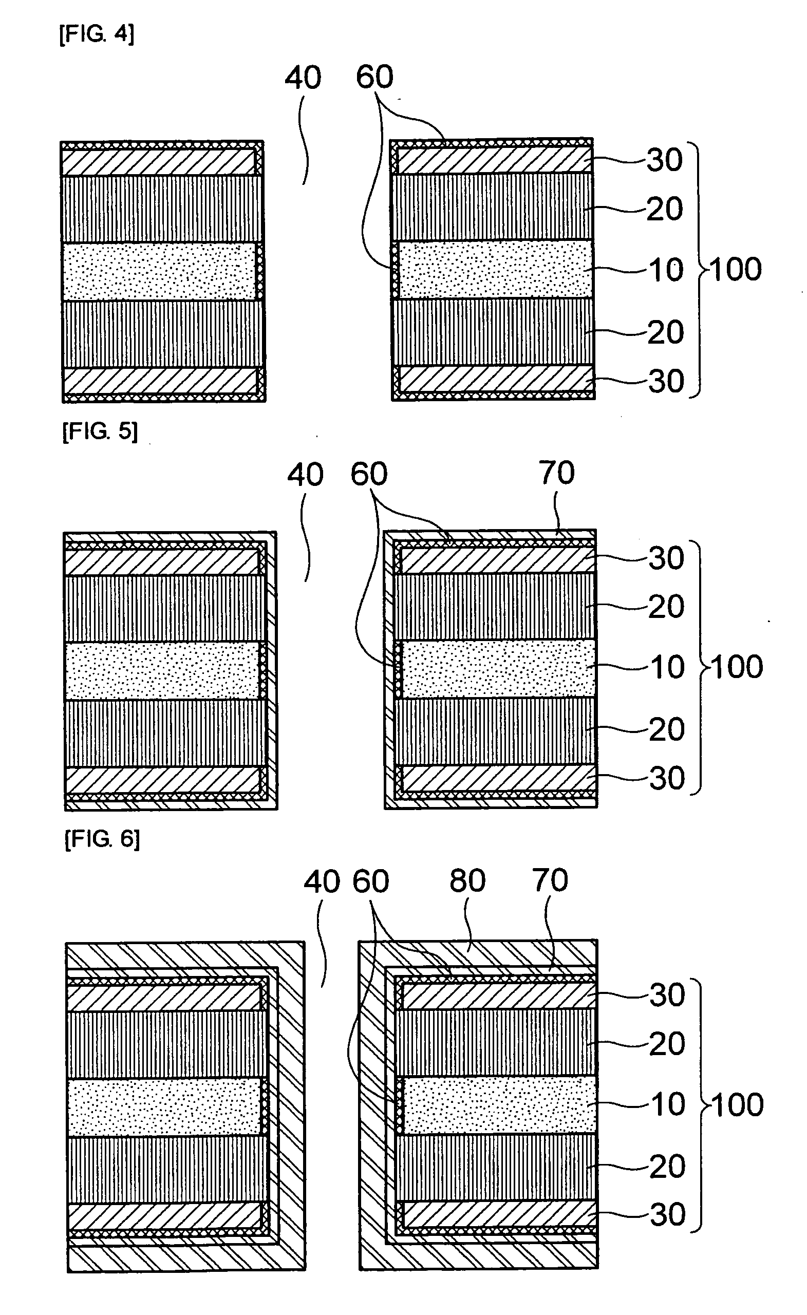
[0038]Referring to FIGS. 1 to 7, a method of manufacturing a PCB according to the invention will be described.

[0039]FIGS. 1 to 7 are process diagrams sequentially showing the method of manufacturing a PCB according to the invention.

[0040]First, as shown in FIG. 1, an aluminum core 10 is provided, and an insulating layer 20 and a copper clad layer 30 are sequentially laminated on and under the aluminum core 10, thereby forming a substrate 100. ...


PUM


Abstract

Provided is a method of manufacturing a PCB, the method comprising: providing a substrate including an aluminum core; forming a via hole passing through the substrate; substituting the surface of the aluminum core with a zinc film by performing a zincate treatment on the inner surface of the via hole; substituting the zinc film with a metal film by performing substitution plating on the zinc film; forming a first plated film on the surface of the via hole, where the metal film is formed, through electroless plating; and forming a second plated film on the first plated film through electroplating.

Description

CROSS-REFERENCE TO RELATED APPLICATIONS[0001]This application claims the benefit of Korean Patent Application No. 10-2008-0041696 filed with the Korea Intellectual Property Office on May 6, 2008, the disclosure of which is incorporated herein by reference.BACKGROUND OF THE INVENTION[0002]1. Field of the Invention[0003]The present invention relates to a method of manufacturing a printed circuit board (PCB) and a PCB manufactured by the same.[0004]2. Description of the Related Art[0005]A PCB is a component for connecting or supporting various electronic parts on a base substrate in accordance with circuit design of electrical wring lines. With the growth of home electronic appliances, communication devices, semiconductor equipments, industrial devices and so on, demand for the PCB is increasing. In particular, as electronic parts are reduced in size, PCB products are also reduced in size and weight.[0006]Currently, the growth of the PCB market in Korea is at a standstill. However, pro...

Claims


Application Information

Patent Timeline
IPC IPC(8): H05K3/42H05K1/11
CPCH05K1/056H05K3/429H05K2203/073H05K2201/09554H05K3/44H05K3/18H05K3/40
Inventor JUNG, HA YONGYANG, DEK GINHEO, CHEOL HOCHUNG, CHAN-YEUPKIM, KEUN HOLEE, SEOUNG JAE
Owner SAMSUNG ELECTRO MECHANICS CO LTD
Why Eureka
Try Eureka