Apparatus and method for column fixed pattern noise (FPN) correction

a column and noise correction technology, applied in the field of image sensors, can solve the problems of inability to correct the offset generated later in the signal processing chain, differences between the circuits in each column, and prone to image artifacts in the cmos iso

Inactive Publication Date: 2009-11-12
ALTASENS
View PDF9 Cites 41 Cited by
  • Summary
  • Abstract
  • Description
  • Claims
  • Application Information

AI Technical Summary

Problems solved by technology

On the other hand, CMOS iSoC's are prone to producing image artifacts that are by-products of the specific analog readout architecture used to capture the image.
All column circuits are designed to be identical, but due to process, voltage, and temperature variations over the sensor, there are differences between the circuits in each column.
While this methodology corrects each column buffer's dc offset, it does not correct offsets generated later in the signal processing chain.
Nevertheless, the '340 patent does not teach specific means and an effective algorithm for correcting FPN.
However, this number of black rows reduces the effective imaging area of the image sensor.

Method used


Image

  • Apparatus and method for column fixed pattern noise (FPN) correction
  • Apparatus and method for column fixed pattern noise (FPN) correction
  • Apparatus and method for column fixed pattern noise (FPN) correction

Examples


Embodiment Construction

[0019]The following description is provided to enable any person skilled in the art to make and use the invention and sets forth the best modes contemplated by the inventor for carrying out the invention. Various modifications, however, will remain readily apparent to those skilled in the art. Any and all such modifications, equivalents and alternatives are intended to fall within the spirit and scope of the present invention.

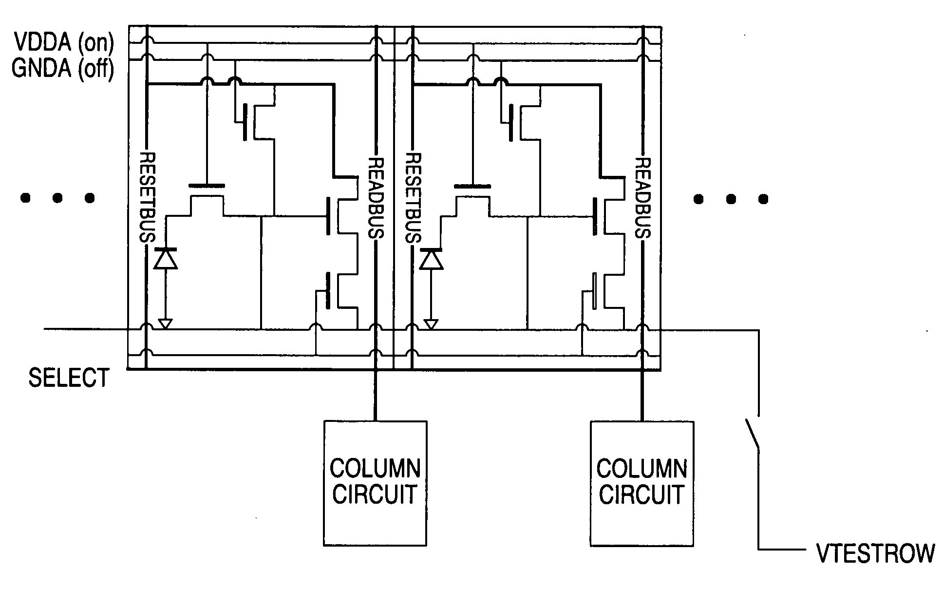
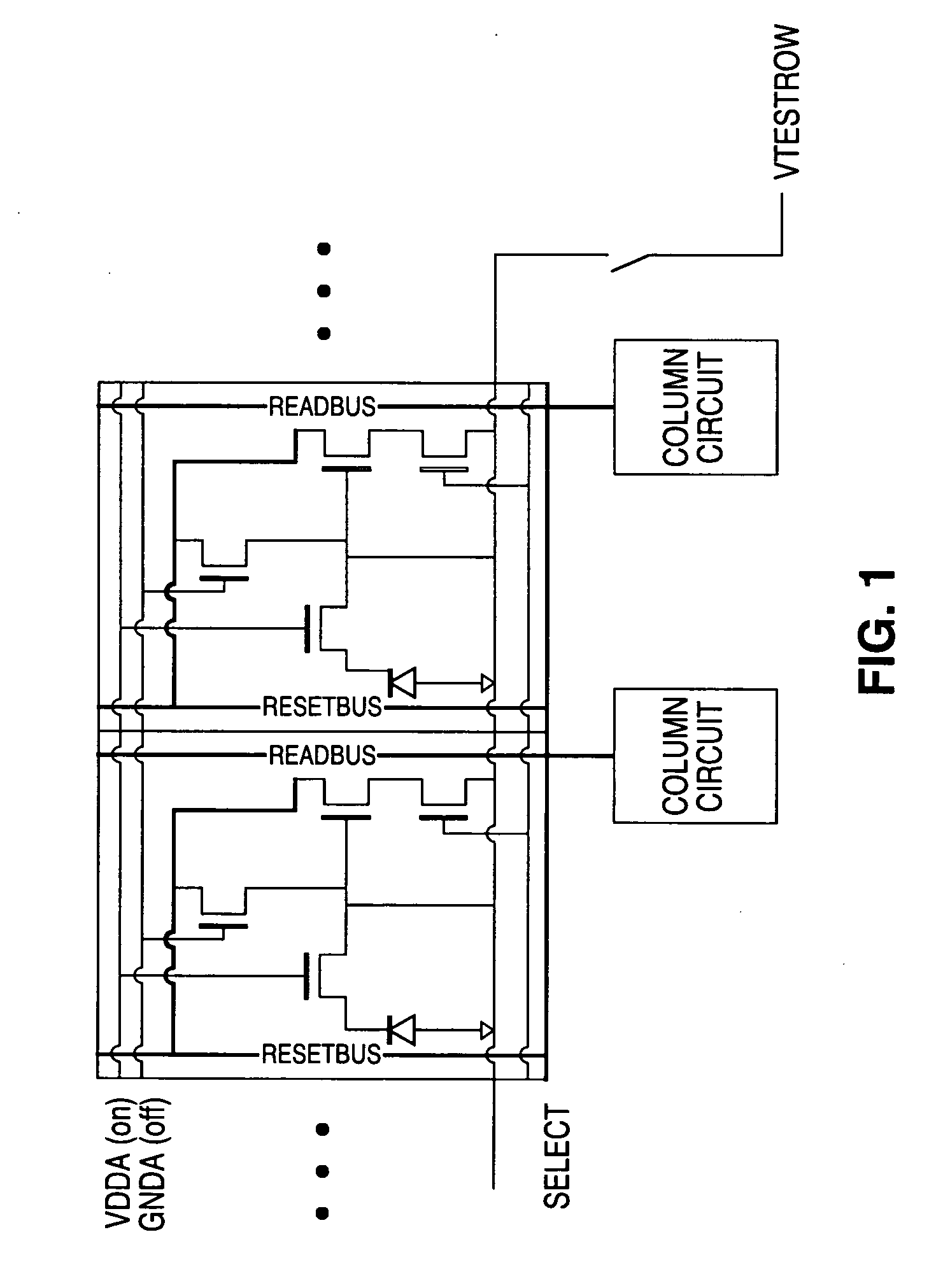
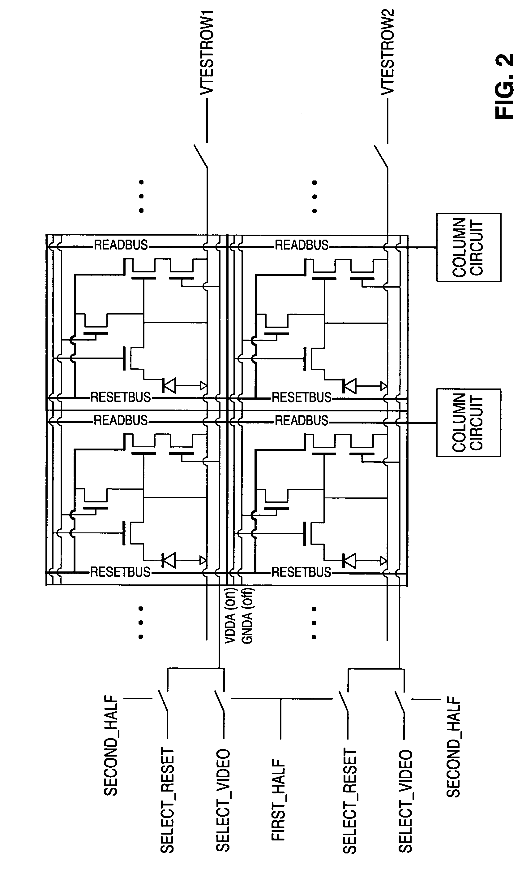
[0020]According to one embodiment of the present invention, a “test row” is repeatedly sampled to determine a column fixed pattern noise (FPN) offset for each column. A test row is a row of pixels whose output does not depend on a photo or dark current signal, but on an externally applied voltage (i.e. a signal external to the pixel array). The voltage may be supplied by a reference voltage on the sensor, from a programmable DAC (Digital-to-Analog Converter), or from a source outside the sensor. The test signal is applied to the floating diffusion in each pixel...


PUM


Abstract

An apparatus and method for fixed pattern noise (FPN) correction in an image sensor utilizes at least one row of test pixels. An external voltage is applied to each pixel circuit in the at least one row. Thus, the output of the test pixels does not depend on the photo or dark current signals. The applied voltage is used to determine a column offset error for each column in the image sensor.

Description

BACKGROUND OF THE INVENTION[0001]1. Field of the Invention[0002]The present invention relates generally to image sensors, and more particularly to an apparatus and method for column fixed pattern noise correction in a CMOS image sensor.[0003]2. Description of the Related Art[0004]Visible imaging systems implemented using CMOS image sensors reduce camera noise, cost and power while simultaneously improving resolution and capture rate. The most advanced and highest performance cameras use CMOS imaging System-on-Chip (iSoC) sensors that efficiently couple low-noise image detection and processing by using various supporting blocks integrated on a single chip.[0005]On the other hand, CMOS iSoC's are prone to producing image artifacts that are by-products of the specific analog readout architecture used to capture the image. A common example of one such image artifact is column Fixed Pattern Noise (FPN), which arises when each column of pixels has a different fixed offset. These offsets a...

Claims


Application Information

Patent Timeline
Patent Type & Authority Applications(United States)
IPC IPC(8): H04N5/217H04N5/365H04N5/374
CPCH04N5/3658H04N25/677
Inventor SHAH, JOEYRICHARDSON, JOHNBLANQUART, LAURENT
Owner ALTASENS
Why Eureka
Try Eureka