Photonic mixer and use thereof

a photonic mixer and mixer technology, applied in the field of photonic mixers, can solve the problems of limiting effects, affecting the diffusion of minority charge carriers, increasing modulation frequency, etc., and achieve the effects of reducing measurement time, reducing the size of the photonic mixer, and increasing resolution

Active Publication Date: 2011-10-20
SOFTKINETIC SENSORS +1
View PDF1 Cites 62 Cited by
  • Summary
  • Abstract
  • Description
  • Claims
  • Application Information

AI Technical Summary

Benefits of technology

[0016]The advantage of the vertical contact is a higher resolution, which may be easily a factor of 10. The higher resolution may be used to provide more individual mixers per unit surface area, or to reduce the size of the photonic mixer.
[0017]In a most relevant embodiment, the photonic mixer is a differential photonic mixer. Thereto, at least two couples of a current injecting contact region and at least one detector region are present within said field area. The advantage of a differential photonic mixer over a photonic mixer with merely one couple, i.e. a single ended photonic mixer, i

Problems solved by technology

It has been found that the provision of these zones leads to an increase in the modulation frequency.
Such undesired presence would hamper the diff

Method used


Image

  • Photonic mixer and use thereof
  • Photonic mixer and use thereof
  • Photonic mixer and use thereof

Examples


first embodiment

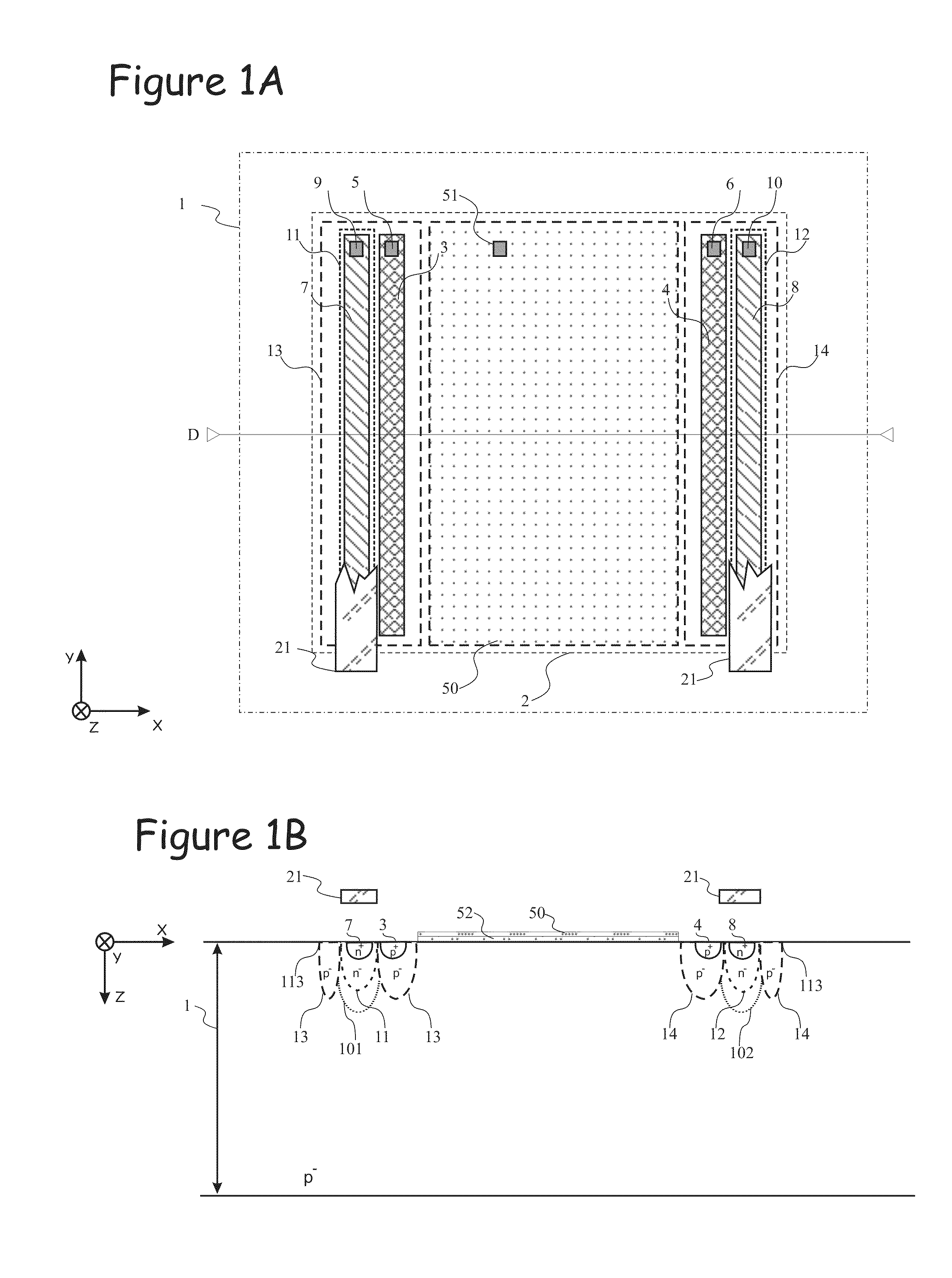
[0046]The top view of FIG. 1A shows the layout of this The field shaping zones 13, 14 are at opposite edges of the field area 2, at which electromagnetic radiation will impinge the substrate so as to be converted into minority and majority carriers. The detector regions 7,8 and the contact regions 3,4 are elongate regions extending parallel to each other and are provided with terminals 9,10 and 5,6 respectively. These terminals 9, 10, 5, 6 are in this example limited to areas at an end of the regions 7, 8, 3, 4 but they not need to be located exactly there. There can be multiple terminals on the same contact region. Masks 21 overlie the detector regions 7,8 in order to shield those from incoming electromagnetic radiation.

second embodiment

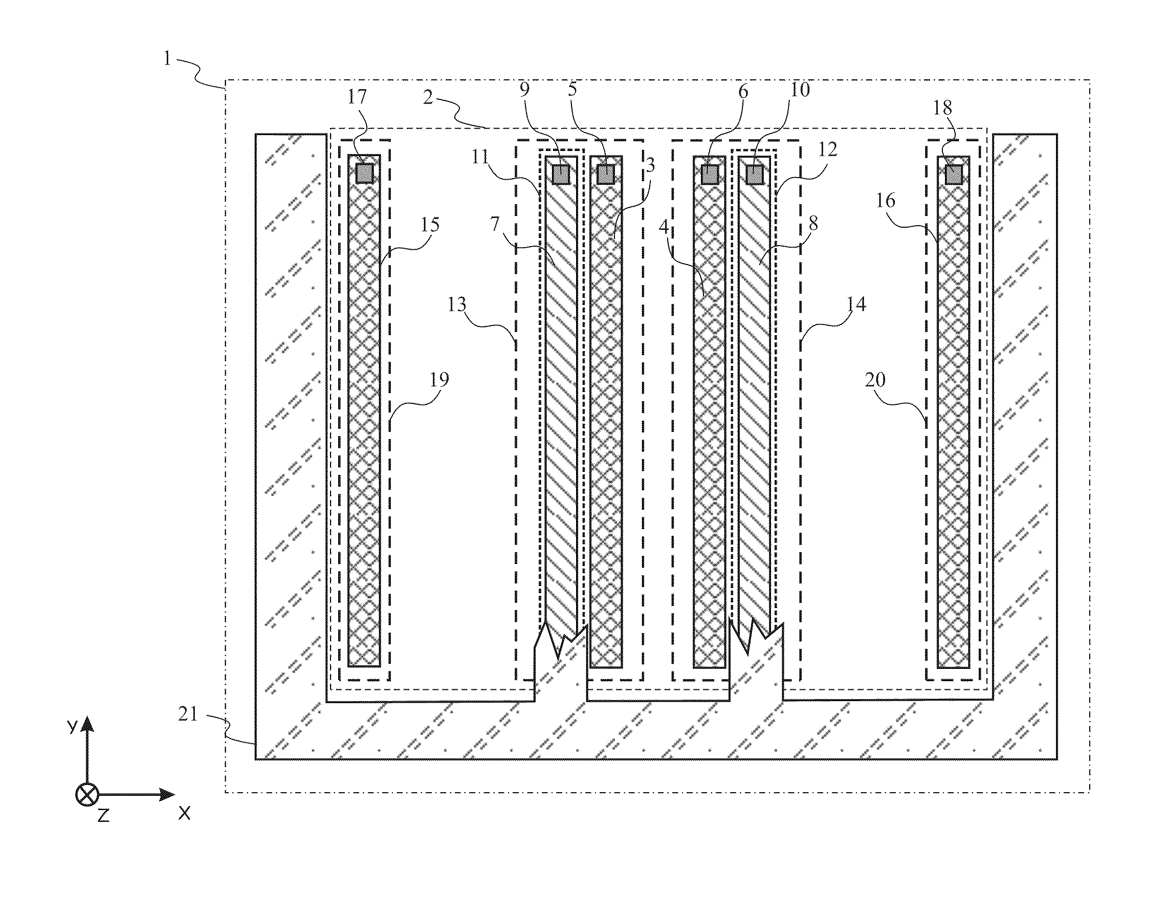
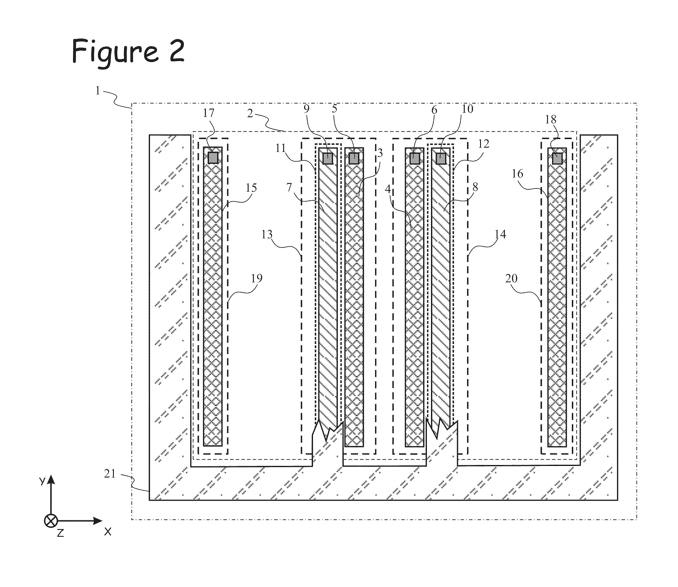
[0047]FIG. 2 is a diagrammatical top view of the invention. Whereas in FIG. 1A, two pairs of a detector region and a contact region are defined at extremes of the field area 2, this embodiment comprises four contact regions 3, 4, 15, 16 and merely two detector regions 7,8. The additional contact regions 15,16 are located at extreme edges of the field area 2. Field shaping zones 19, 20 are defined below the additional contact regions 15, 16 and terminals 17, 18 are defined thereon. The additional contact regions 15,16 are designed to be put on a constant voltage during the photonic mixing operation. The contact regions 3,4 are intended to be put on alternating voltages. Therewith, one may apply a field with both a AC component and a DC component. The application of such field is found to limit crosstalk.

[0048]It is an option of the present embodiment to leave out one of the detector regions 7,8. That is beneficial so as to reduce detector area for smaller devices. This option is not ...


PUM


Abstract

The photonic mixer comprises a couple of an injecting contact region (3,4) for injecting the majority carrier current into the semiconductor substrate (1) and a detector region (7,8) for collecting the photocurrent. The injecting contact region (3,4) is doped with a dopant of the first conductivity type (p+) at a higher dopant concentration than the semiconductor substrate (1). The detector region (7,8) is doped with a dopant of a second conductivity type (n+) opposite the first conductivity type and has a junction (11,12) with the semiconductor substrate (1), a zone of the semiconductor substrate (1) around said junction (11,12) being a depleted substrate zone (101, 102). The couple further comprises a field shaping zone (13, 14) of the first conductivity type (p) defining a lateral edge of the couple and having a dopant concentration higher than the dopant concentration of the semiconductor substrate (1), for example between the dopant concentrations of the semiconductor substrate (1) and the injecting contact region (3,4), which field shaping zone (13, 14) is designed to limit said depleted substrate zone (101, 102) laterally.

Description

TECHNICAL FIELD OF THE INVENTION[0001]The invention relates to a photonic mixer provided with a semiconductor substrate having a field area and means for generating a majority carrier current and an associated electric field in the semiconductor substrate that is doped with a first conductivity type, such that when electromagnetic radiation impinges on the substrate within said field area, pairs of majority and minority carriers are generated in the substrate, resulting in a photocurrent of the minority carriers, said substrate comprising:[0002]at least one injecting contact region of the first conductivity type for generating the majority carrier current and the associated electric field by injecting the majority carrier current into the semiconductor substrate, said contact region having a higher dopant concentration than the semiconductor substrate, and[0003]at least one detector region of a second conductivity type opposite to the first conductivity type for collecting the photo...

Claims


Application Information

Patent Timeline
IPC IPC(8): G01C3/08H01L27/148G01S7/4913
CPCG01S7/4913H01L27/14609H01L31/103G01S17/06H01L31/101G01S7/487H01L31/0352H01L31/035272
Inventor VAN DER TEMPEL, WARDVAN NIEUWENHOVE, DANIELKUIJK, MAARTEN
Owner SOFTKINETIC SENSORS
Why Eureka
Try Eureka