Silicon interposer and method for manufacturing the same

a technology of silicon interposer and silicon plate, which is applied in the direction of semiconductor/solid-state device details, semiconductor devices, electrical devices, etc., can solve the problems of large aspect ratio, difficult to form uniformly an insulating film on through holes, and great thermal stress between semiconductor elements and mounting substrates

Active Publication Date: 2009-11-19
SHINKO ELECTRIC IND CO LTD
View PDF3 Cites 34 Cited by
  • Summary
  • Abstract
  • Description
  • Claims
  • Application Information

AI Technical Summary

Benefits of technology

[0009]Illustrative aspects of the present invention provide a silicon interposer capable of providing electrical insulation between through electrodes and a silicon subst

Problems solved by technology

When the semiconductor element that produces heat in operation is mounted on the mounting substrate, a great thermal stress is caused between the semiconductor element and the mounting substrate.
A method for forming a protection film by the low-temperature CVD method has such an advantage that the ele

Method used


Image

  • Silicon interposer and method for manufacturing the same
  • Silicon interposer and method for manufacturing the same
  • Silicon interposer and method for manufacturing the same

Examples


Embodiment Construction

(Silicon Interposer Manufacturing Method)

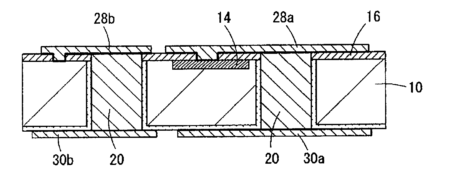
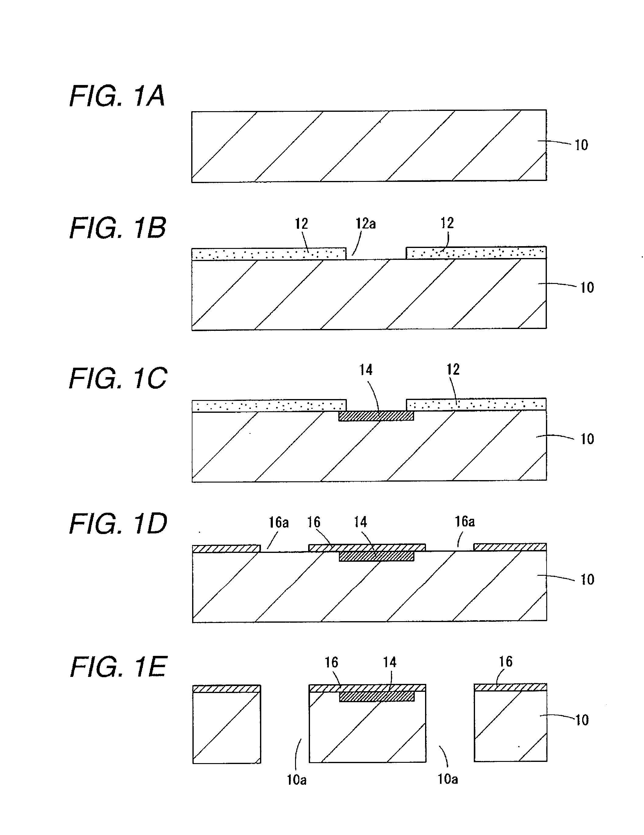
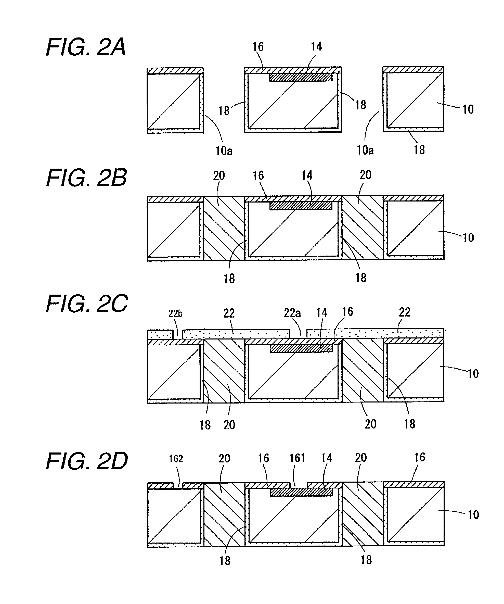
[0023]FIGS. 1A to 1E show steps required until forming an element portion on a surface of a silicon wafer 10 serving as a base material of a silicon interposer by forming an impurity diffusing layer, and then forming through holes used to form through electrodes in the silicon wafer 10.

[0024]FIG. 1A shows the silicon wafer 10, and FIG. 1B shows a state that a resist pattern 12 used to form the element portion is formed on a surface of the silicon wafer 10. A large number of silicon interposers are formed from a sheet of silicon wafer 10. The resist pattern 12 is patterned every unit area of the silicon interposers, which are formed on the silicon wafer 10, to meet an arrangement of the elements portions. Here, constituent portions of the silicon interposer as one unit constituting the silicon wafer 10 are shown in following FIGS. 1C to 1E.

[0025]FIG. 1C shows a state that an element portion 14 formed of an impurity diffusing layer is formed by...


PUM


Abstract

A method for manufacturing a silicon interposer, includes a step of forming a protection film on a surface, on which an element portion is formed, of a silicon wafer, a step of forming open holes according to planar arrangements of through holes which pass through the silicon wafer in a thickness direction, a step of forming the through holes by etching the silicon wafer using the protection film as a mask, a step of forming an oxide film on inner wall surfaces of the through holes by a thermal oxidation, a step of forming a contact hole, which is in communication with the element portion, in the protection film, and a step of forming wirings on both surfaces of the silicon wafer. In the step of forming the wirings, one of the wirings is formed to be connected electrically to the element portion via a contact portion formed in the contact hole.

Description

[0001]This application claims priority from Japanese Patent Application No. 2008-127918, filed on May 15, 2008, the entire contents of which are hereby incorporated by reference.FIELD OF THE INVENTION[0002]The present disclosure relates to a silicon interposer and a method for manufacturing the same and, more particularly, a silicon interposer in which an element portion such as a diode is formed on a surface of a silicon substrate and a method for manufacturing the same.DESCRIPTION OF RELATED ART[0003]The silicon interposer is interposed between a semiconductor element and a mounting substrate, and electrically connects the mounting substrate and the semiconductor element. A coefficient of thermal expansion is very different between the semiconductor element and the mounting substrate made of a resin substrate. When the semiconductor element that produces heat in operation is mounted on the mounting substrate, a great thermal stress is caused between the semiconductor element and t...

Claims


Application Information

Patent Timeline
IPC IPC(8): H01L23/48H01L21/768
CPCH01L21/486H01L23/147H01L2924/12041H01L23/481H01L23/49827H01L23/60H01L24/16H01L24/81H01L25/18H01L33/62H01L2224/81192H01L2224/81205H01L2224/81801H01L2224/8383H01L2924/01029H01L2924/01078H01L2924/01079H01L2924/10253H01L2924/19041H01L2924/19043H01L2924/01005H01L2924/01006H01L2924/01033H01L2924/00H01L2224/05568H01L2224/05573H01L2224/05644H01L2924/12035H01L2924/351H01L2924/00014
Inventor MURAYAMA, KEI
Owner SHINKO ELECTRIC IND CO LTD
Why Eureka
Try Eureka