Methods of fabricating an array capacitor

a technology of array capacitors and array capacitors, which is applied in the direction of variable capacitors, fixed capacitor details, fixed capacitors, etc., can solve the problems of increased mechanical stress on the via structure, high propensity to form tapered via holes, and difficulty in fabricating thick array capacitors

Inactive Publication Date: 2009-11-26
INTEL CORP
View PDF9 Cites 3 Cited by
  • Summary
  • Abstract
  • Description
  • Claims
  • Application Information

AI Technical Summary

Problems solved by technology

Fabrication of thick array capacitors, e.g. having a thickness of about 1000 μm and above, has been fraught with difficulties.
One reason is the high propensity to form tapered via holes due to limitations of current hole-drilling methods.
Other disadvantages of having tapered vias, and voids in the via structures include increased mechanical stress to the via structures and undesirable variations in Equivalent Series Resistance and Equivalent Series Inductance of an array capacitor.
These voids are undesirable as they constrict electrical current flow and thereby increase electrical resistance of the via structures.
Several fabrication methods have been devised in at

Method used


Image

  • Methods of fabricating an array capacitor
  • Methods of fabricating an array capacitor
  • Methods of fabricating an array capacitor

Examples


Embodiment Construction

[0011]In the following description, numerous specific details are set forth in order to provide a thorough understanding of various illustrative embodiments of the present invention. It will be understood, however, to one skilled in the art, that embodiments of the present invention may be practiced without some or all of these specific details. In other instances, well known process operations have not been described in detail in order not to unnecessarily obscure pertinent aspects of embodiments being described. In the drawings, like reference numerals refer to same or similar functionalities or features throughout the several views.

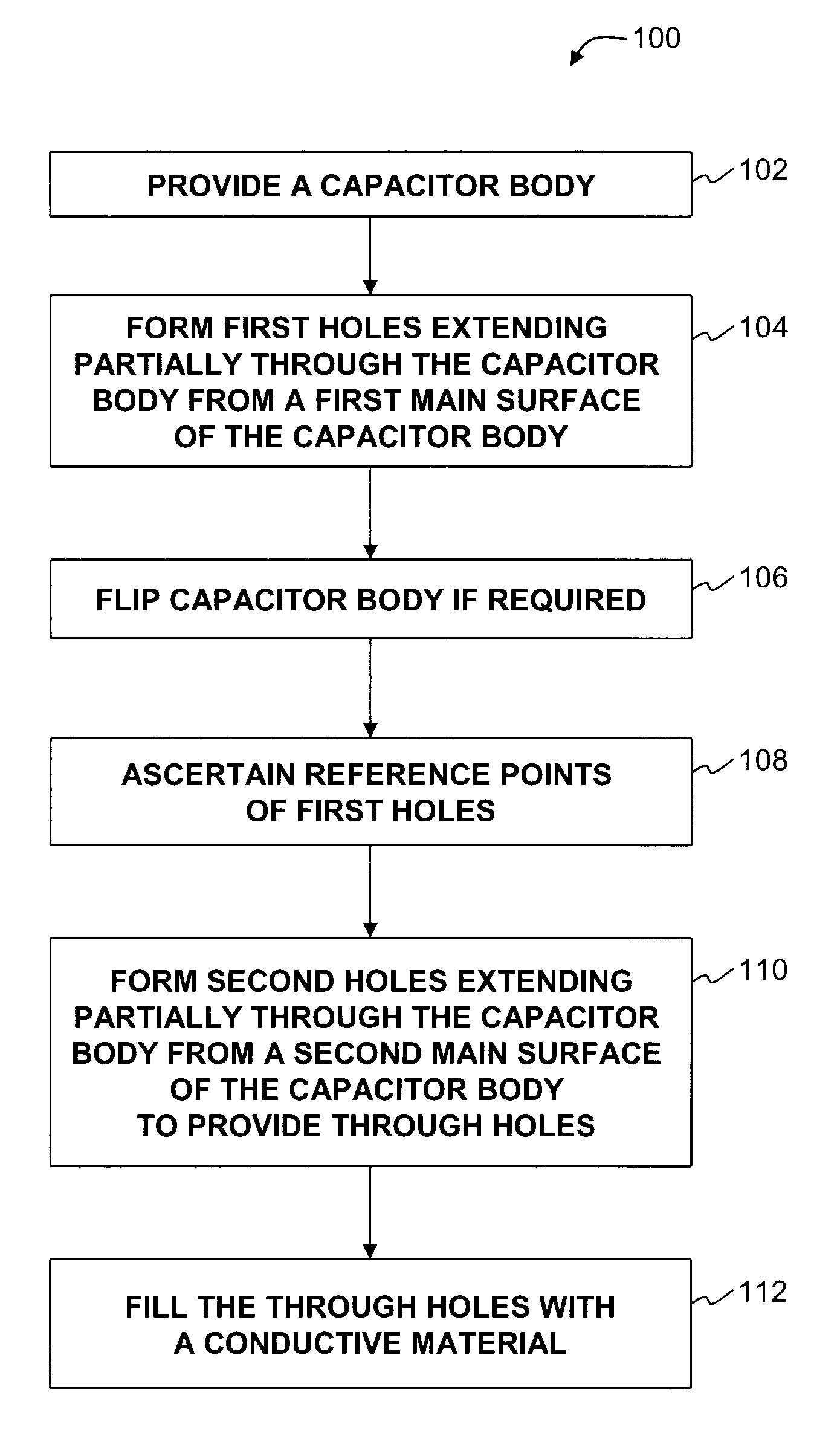
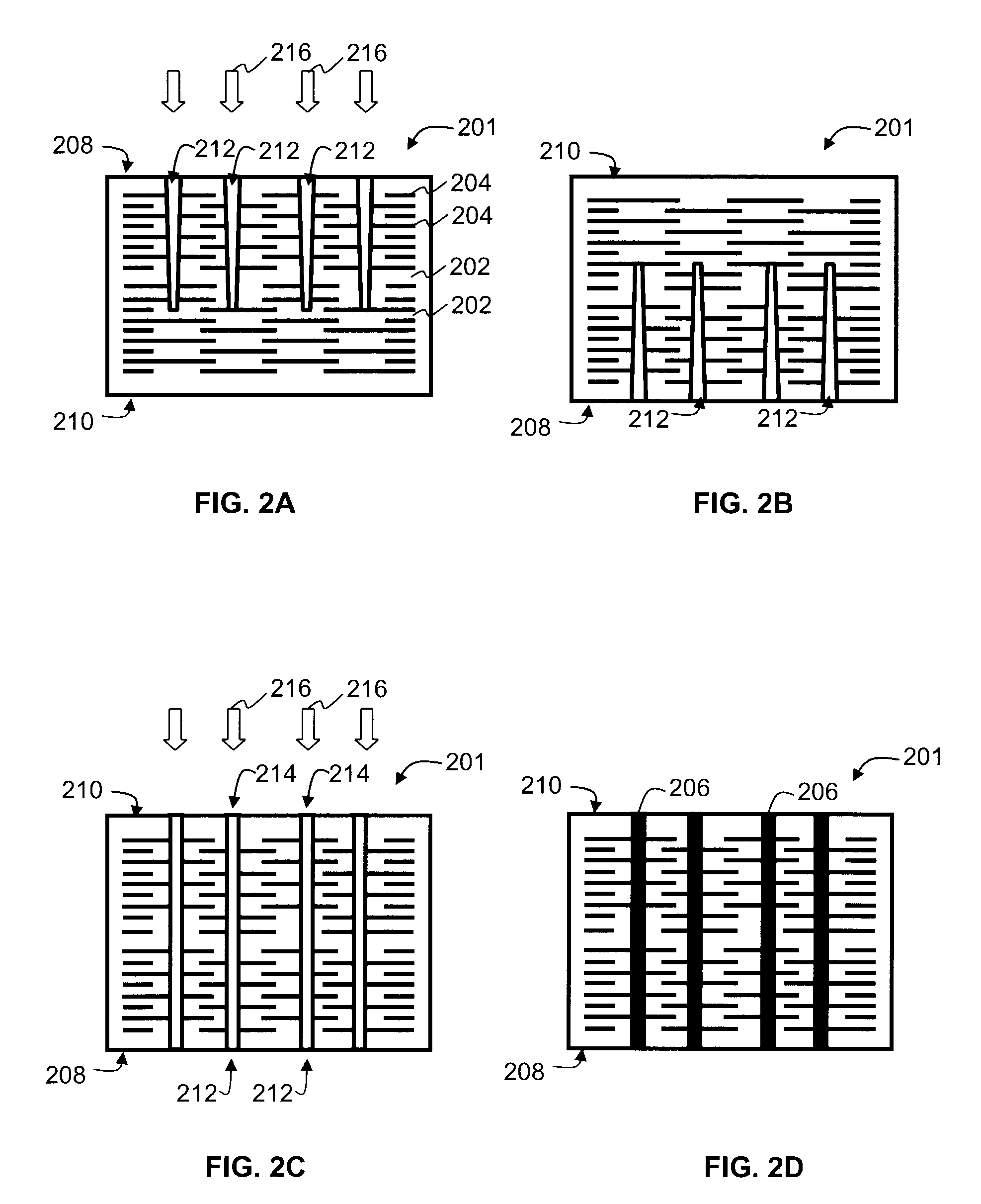
[0012]FIG. 1 is a flow chart summarizing a sequence 100 of fabricating an array capacitor according to one embodiment of the invention. The process sequence 100 will be described with further reference to FIGS. 2A to 2D illustrating various process outputs obtained during the process sequence 100 of FIG. 1.

[0013]The process sequence 100 begins with pro...


PUM

PropertyMeasurementUnit
Fractionaaaaaaaaaa
Thicknessaaaaaaaaaa
Thicknessaaaaaaaaaa

Abstract

Methods of fabricating an array capacitor are disclosed, in which via structures of the array capacitor have increased uniformity in their transverse areas. One method involves perforating a capacitor body to form first holes extending from a first surface and partially through the capacitor body. The capacitor body may be further perforated to form second holes extending from a second opposed surface of the capacitor body. The second holes are to connect to the first holes to provide through holes extending across a thickness of the capacitor body. An appropriate conductive material may then be filled in the through holes to form via structures with increased uniformity in their transverse areas.

Description

BACKGROUND[0001]1. Technical Field[0002]Embodiments of the invention relate to array capacitors for electronic packages, and more particularly to methods of fabricating an array capacitor.[0003]2. Description of Related Art[0004]Fabrication of thick array capacitors, e.g. having a thickness of about 1000 μm and above, has been fraught with difficulties. One reason is the high propensity to form tapered via holes due to limitations of current hole-drilling methods. Other disadvantages of having tapered vias, and voids in the via structures include increased mechanical stress to the via structures and undesirable variations in Equivalent Series Resistance and Equivalent Series Inductance of an array capacitor. Due to tapering of the via holes, voids are formed upon filling the via holes. These voids are undesirable as they constrict electrical current flow and thereby increase electrical resistance of the via structures.[0005]Several fabrication methods have been devised in attempts t...

Claims


Application Information

Patent Timeline
IPC IPC(8): H01G7/00
CPCH01G4/232H01G4/30H01G4/38Y10T29/12Y10T29/43Y10T29/417Y10T29/435
Inventor DATTAGURU, SRIRAM
Owner INTEL CORP
Why Eureka
Try Eureka