Light emitting device and method of manufacturing light emitting device

a technology of light emitting device and light emitting device, which is applied in the direction of solid-state devices, lasers, semiconductor lasers, etc., can solve the problems of difficult size reduction, inferior hermetic sealing performance, and difficult mass productivity, so as to achieve the effect of improving hermetic sealing performance and mass productivity

Inactive Publication Date: 2009-12-03
SONY CORP
View PDF2 Cites 28 Cited by
  • Summary
  • Abstract
  • Description
  • Claims
  • Application Information

AI Technical Summary

Benefits of technology

[0012]The CAN package which is mainstream in the optical disc application has a disadvantage in mass productivity in a point that the manufacturing method is not a batch method. Though the CAN package has an advantage that heat releasing performance and hermetic sealing performance after assembly can be secured, it is difficult to realize size reduction. On the other hand, a frame laser in which the substrate to which the light emitting element is connected is made of resin is suitable for realizing size reduction, but is inferior in the hermetic sealing performance because the material is resin.

Problems solved by technology

The CAN package which is mainstream in the optical disc application has a disadvantage in mass productivity in a point that the manufacturing method is not a batch method.
Though the CAN package has an advantage that heat releasing performance and hermetic sealing performance after assembly can be secured, it is difficult to realize size reduction.
On the other hand, a frame laser in which the substrate to which the light emitting element is connected is made of resin is suitable for realizing size reduction, but is inferior in the hermetic sealing performance because the material is resin.
In the light emitting device in which the light emitting element is mounted on the support substrate in the lateral posture, there was a problem that hermetic sealing performance is low due to surface inaccuracy of the window attaching surface.
For example, in the case that solder is used as an adhesive when attaching the light exiting window, flatness of a soldering surface deteriorates due to effects of surface tension when the solder is melted because of the surface inaccuracy of the window attaching surface.
Accordingly, unevenness in thickness occurs in a solder layer and a gap may be generated after the solder is solidified due to the unevenness.
As a result, it is difficult to seal the light emitting element with high hermeticity.
Furthermore, considering positioning accuracy in a stacking process, variations in size due to difference between solidification and contraction in respective layers and the like, it is assumed that the surface accuracy of the window attaching surface further deteriorates.
Therefore, it is difficult to secure high hermetic sealing performance by using a solder glass and the like.
First of all, since the stacking process is necessary, there is an disadvantage in points of deterioration of productivity and cost increase caused by increase of the number of processes.

Method used


Image

  • Light emitting device and method of manufacturing light emitting device
  • Light emitting device and method of manufacturing light emitting device
  • Light emitting device and method of manufacturing light emitting device

Examples


first embodiment

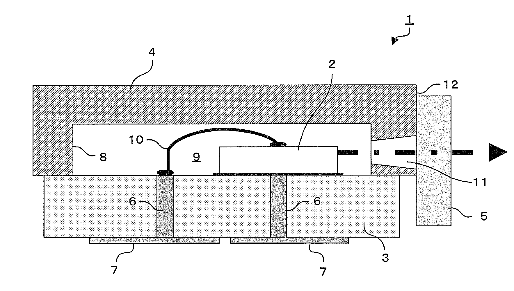
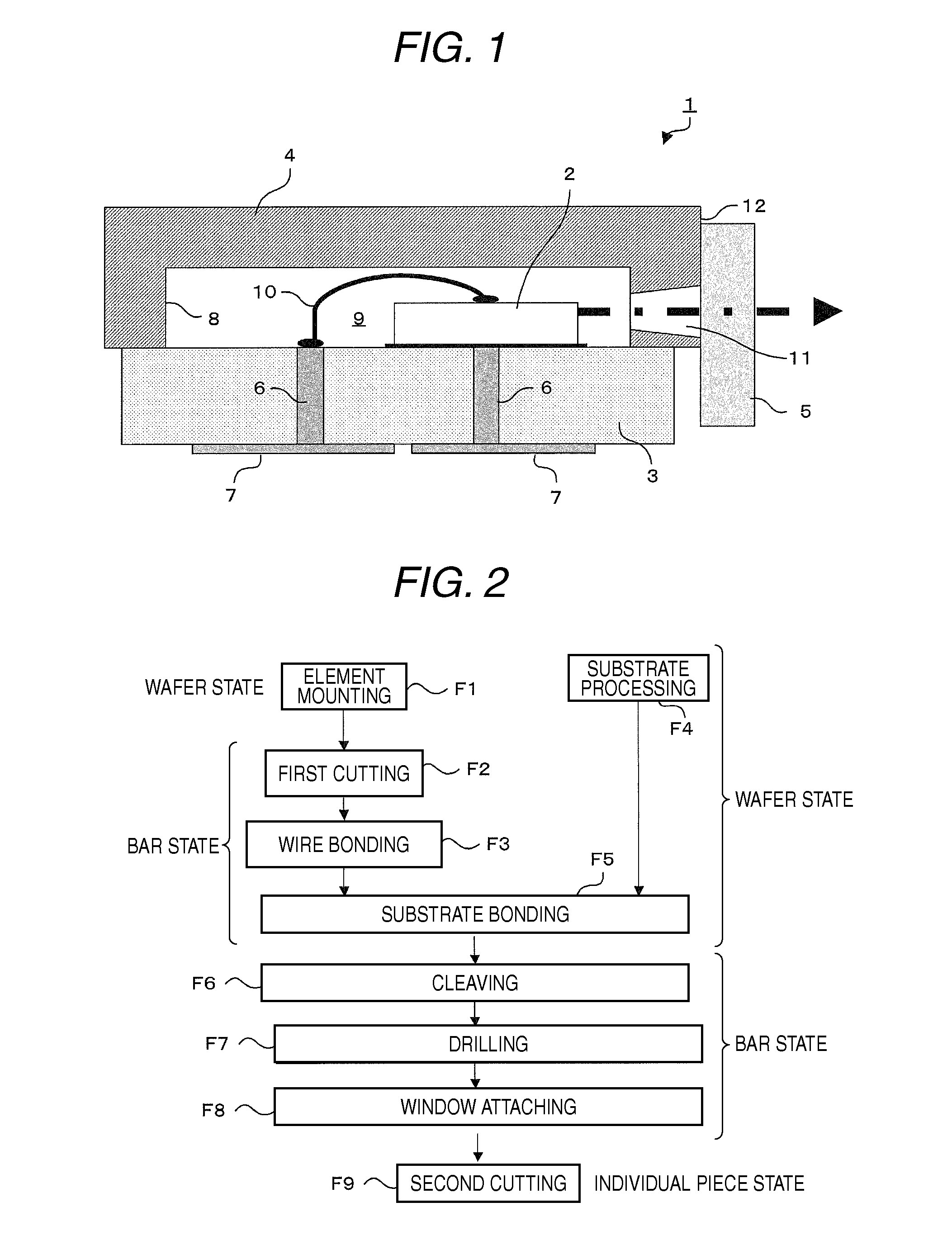
[0036]FIG. 1 is a sectional side view showing a configuration of a light emitting device according to a first embodiment of the invention. A shown light emitting device 1 largely includes a light emitting element 2, a first substrate 3, a second substrate 4 and a light exiting window 5.

[0037]The light emitting element 2 is formed by using, for example, a semiconductor light emitting element such as a semiconductor laser. In the light emitting element 2, light is emitted in a direction of an arrow (right direction) in the drawing. The light emitting element 2 is an element having light emitting wavelength of, for example, 450 nm or less, and particularly, when used as a light source for a Blu-ray disc, an element having a light emitting wavelength of 405 nm is used. Incidentally, in a light source for a DVD, an element having a light emitting wavelength of 650 nm is used. The light emitting element 2 is bonded to an upper surface of the first substrate 3 by using, for example, solder...

second embodiment

[0060]FIG. 8 is a sectional side view showing a configuration of a light emitting device according to a second embodiment of the invention. In the second embodiment of the invention, explanation will be made by putting the same numerals on corresponding components cited in the first embodiment. The shown light emitting device 1 largely includes the light emitting element 2, the first substrate 3, the second substrate 4 and the light exiting window 5, which is the same as the first embodiment in this point. However, the second embodiment is different from the first embodiment in the following points.

[0061]Specifically, in the first embodiment, the first substrate 3 is formed by using an AlN substrate not having cleavage characteristics. On the other hand, in the second embodiment, the first substrate 3 is formed by using a silicon substrate having cleavage characteristics. According to this, in the second embodiment, both the first substrate 3 and the second substrate 4 are formed by...


PUM


Abstract

A light emitting device includes a light emitting element emitting light, a first substrate on which the light emitting element is mounted, a second substrate forming a sealing space for the light emitting element between the first substrate and the second substrate and a light exiting window for allowing light emitted from the light emitting element to exit, in which at least one of the first substrate and the second substrate has cleavage characteristics and a cleavage plane thereof serves as a window attaching surface to which the light exiting window is attached.

Description

BACKGROUND OF THE INVENTION[0001]1. Field of the Invention[0002]The present invention relates to a light emitting device and a method of manufacturing the light emitting device. Particularly, the invention relates to a light emitting device (semiconductor light emitting device) including a semiconductor light emitting element typified by a semiconductor laser and a method of manufacturing the same.[0003]2. Description of the Related Art[0004]A package of a semiconductor laser is commonly made of a metal material called as a CAN package. The size of the package for a light source of an optical disc was mainly 9 mm in diameter in 1980's, 5.6 mm in diameter in 1990's and is 3 mm in one edge in 2000's, which is made of a resin material called as a frame. In the present circumstances, further size reduction of the package is demanded. On the background thereof, there is a demand for a thinner and smaller optical disc device (recording / playback device) which uses the semiconductor laser a...

Claims


Application Information

Patent Timeline
Patent Type & Authority Applications(United States)
IPC IPC(8): H01L33/00H01L21/77H01L33/48H01L33/62H01S5/022
CPCH01S5/0202H01S5/02216H01L2224/48479H01L2224/48471H01L2224/48227H01L24/97H01L2924/3025H01S5/02272H01S5/02276H01S5/02292H01L2224/45144H01L2924/00H01L2924/00014H01L2924/15788H01S5/02255H01S5/02345H01S5/0237H01L2224/4554
Inventor YOSHIDA, HIROSHI
Owner SONY CORP
Why Eureka
Try Eureka