SRAM memory cell having transistors integrated at several levels and the threshold voltage vt of which is dynamically adjustable

Active Publication Date: 2009-12-03
COMMISSARIAT A LENERGIE ATOMIQUE ET AUX ENERGIES ALTERNATIVES
View PDF12 Cites 168 Cited by
  • Summary
  • Abstract
  • Description
  • Claims
  • Application Information

AI Technical Summary

Benefits of technology

[0023]A cell such as this has both improved integration density and electrical perfo

Problems solved by technology

4T cells have the disadvantage of having a lack of stability in retention mode.
This results in an increase in the sensitivity of the memory cells to various noise sources.
These cells do not enable a h

Method used


Image

  • SRAM memory cell having transistors integrated at several levels and the threshold voltage vt of which is dynamically adjustable
  • SRAM memory cell having transistors integrated at several levels and the threshold voltage vt of which is dynamically adjustable
  • SRAM memory cell having transistors integrated at several levels and the threshold voltage vt of which is dynamically adjustable

Examples


Embodiment Construction

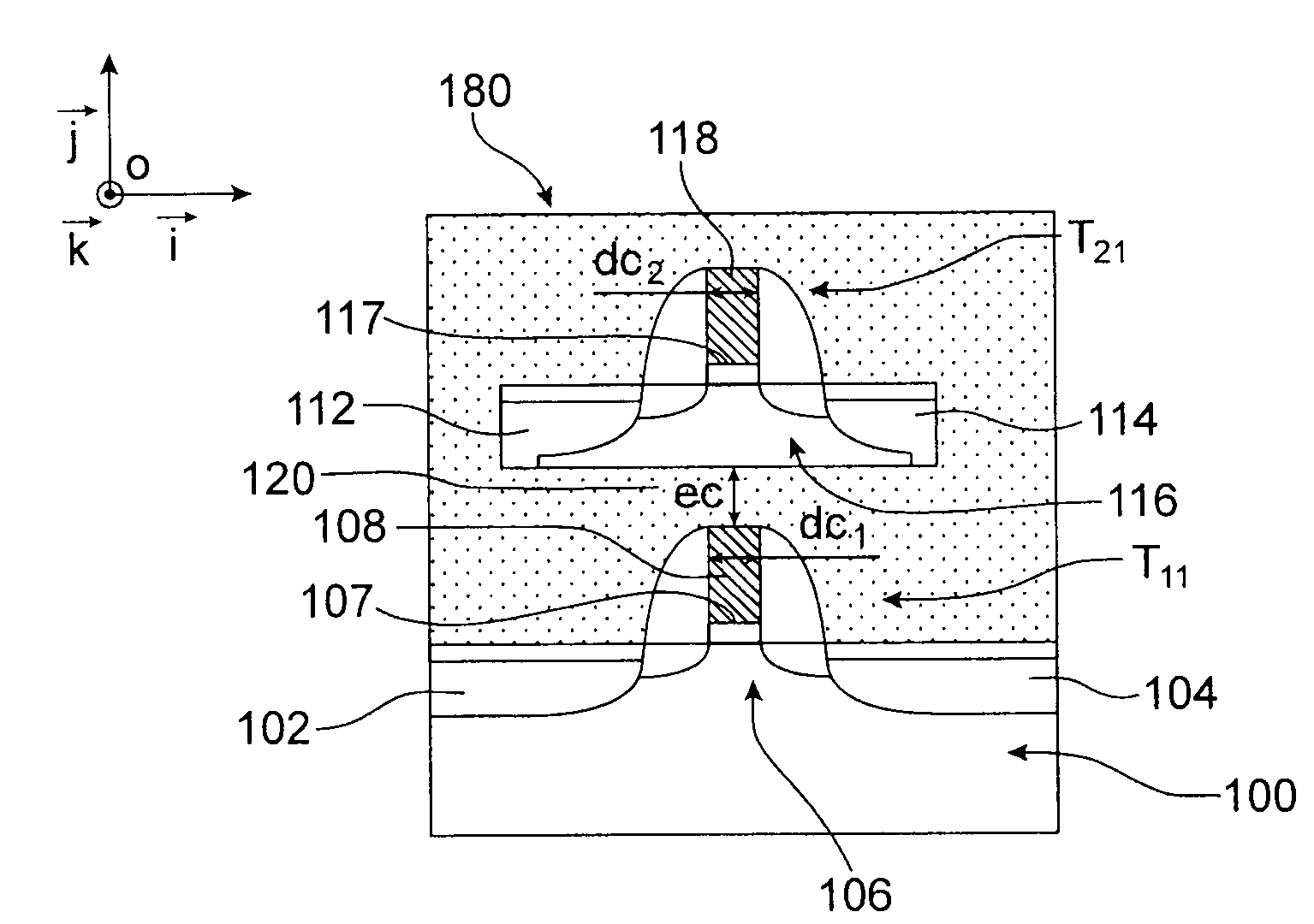
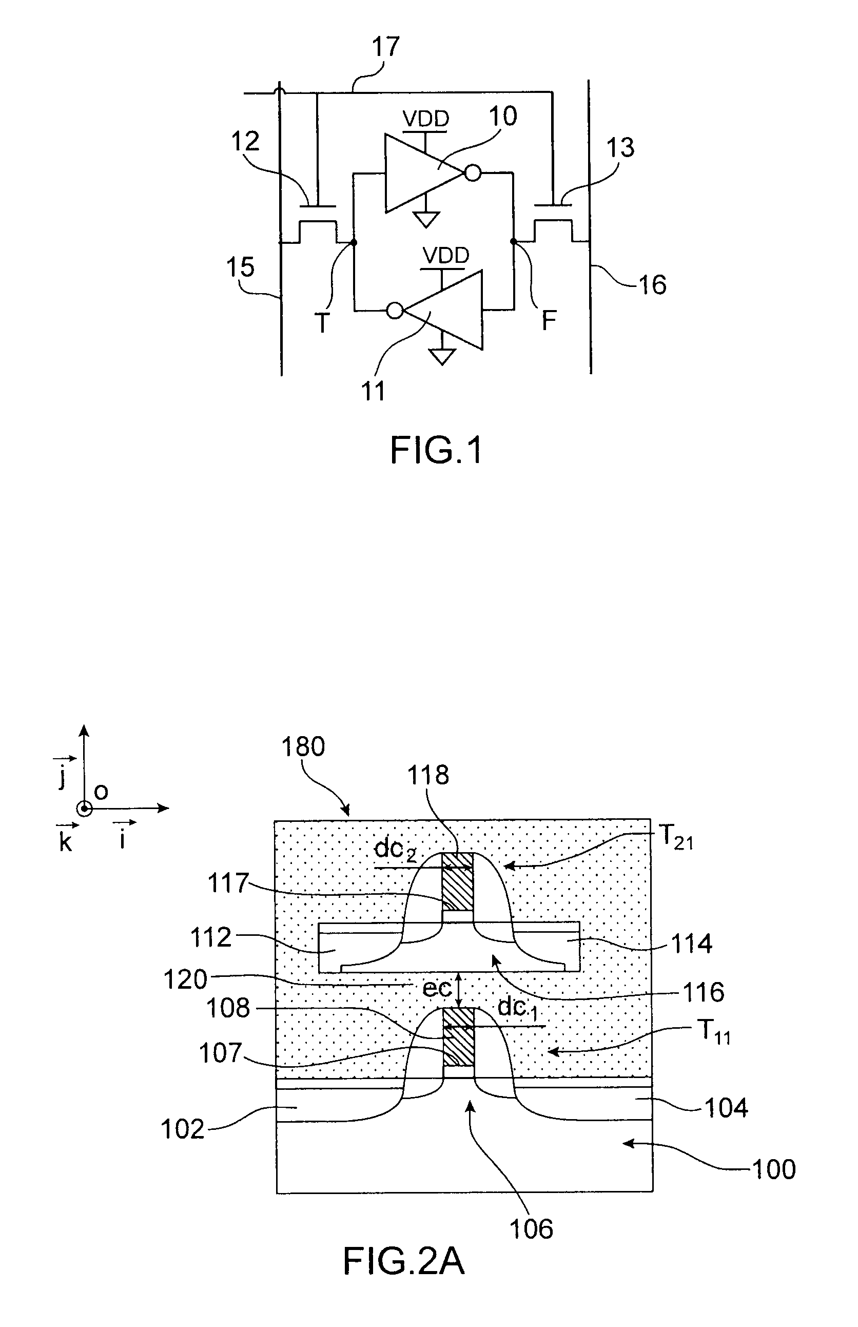
[0049]A transistor arrangement, as anticipated in a memory cell implemented according to the invention, will now be provided in connection with FIG. 2A.

[0050]The transistors are produced on a substrate 100, which can be a bulk or semiconductor-on-insulator type substrate, e.g., of the SOI (silicon-on-insulator) type, comprising a first support layer which can be semi-conducting and, for example, containing Si, which is coated with an insulating layer, e.g., containing SiO2, which is itself coated with a semiconductor layer, e.g., containing Si, and in which one or more active regions are capable of being formed.

[0051]A stack of layers rests on the substrate 100, in which a first transistor T1l appears, comprising a source region 102, a drain region 104, as well as a channel region 106 connecting the source region 102 and the drain region 104. The first transistor T11 may optionally be formed on a completely depleted or partially depleted SOI substrate.

[0052]The transistor T11 likewi...


PUM


Abstract

A non-volatile random access memory cell which, on a substrate surmounted by a stack of layers, comprises:
a first plurality of transistors situated at a given level of the stack of which at least one first access transistor and at least one second access transistor, which are arranged between a first bit line and a first storage node, and between a second bit line and a second storage node, respectively, the first access transistor and the second access transistor having a gate connected to a word line,
a second plurality of transistors forming a flip-flop and situated at, at least one other level of the stack, beneath said given level,
the transistors of the second plurality of transistors each comprising a gate electrode situated opposite a channel region of a transistor of the first plurality of transistors and separated from this channel region by means of an insulating region provided to enable coupling of said gate electrode and said channel region.

Description

TECHNICAL FIELD[0001]This invention relates to the field of memories, and in particular to that of static random access memories SRAM (RAM for “random access memory”). The invention relates in particular to an improved memory cell provided with stacked transistors of which a plurality of transistors have a threshold voltage that can be modulated by coupling with the lower transistor gate.[0002]It introduces advantages particularly in terms of overall dimensions, and the possibility of dynamically modifying the threshold voltage of some of the transistors so as to improve the electrical characteristics thereof, such as stability and consumption.PRIOR ART[0003]A conventional SRAM memory cell (SRAM for “static random access memory” or static RAM) generally includes two inverters 10, 11, which are connected in a so-called “bistable” or “flip-flop” configuration, and two access transistors 12, 13, which are connected to bit lines 15 and 16 and controlled by a word line 17 (FIG. 1).[0004]...

Claims


Application Information

Patent Timeline
IPC IPC(8): H01L27/11
CPCH01L27/0688H01L27/11H01L27/1203H01L27/1108H01L27/1104H10B10/125H10B10/00H10B10/12
Inventor THOMAS, OLIVIERBATUDE, PERRINEPOUYDEBASQUE, ARNAUDVINET, MAUD
Owner COMMISSARIAT A LENERGIE ATOMIQUE ET AUX ENERGIES ALTERNATIVES
Why Eureka
Try Eureka