

Semiconductor device and manufacturing method therefor
a semiconductor device and manufacturing method technology, applied in the direction of semiconductor devices, semiconductor/solid-state device details, electrical apparatus, etc., can solve the problem of reducing the outer dimensions of (downsize and thin) electronic equipment, and achieve the effect of reducing the mounting height of the semiconductor devi
- Summary
- Abstract
- Description
- Claims
- Application Information
AI Technical Summary
Benefits of technology
Problems solved by technology
Method used
Image

Examples
first embodiment
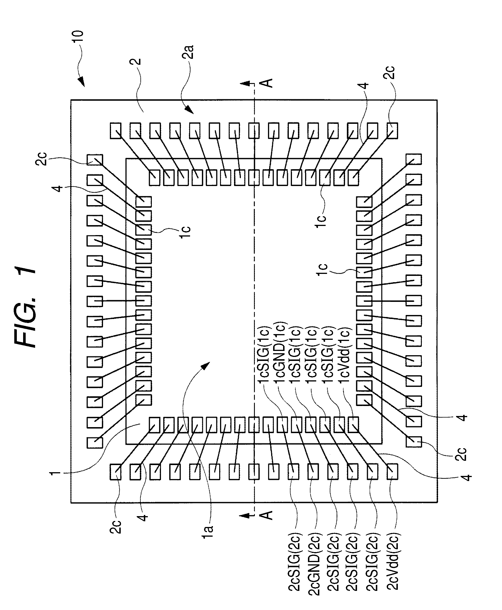
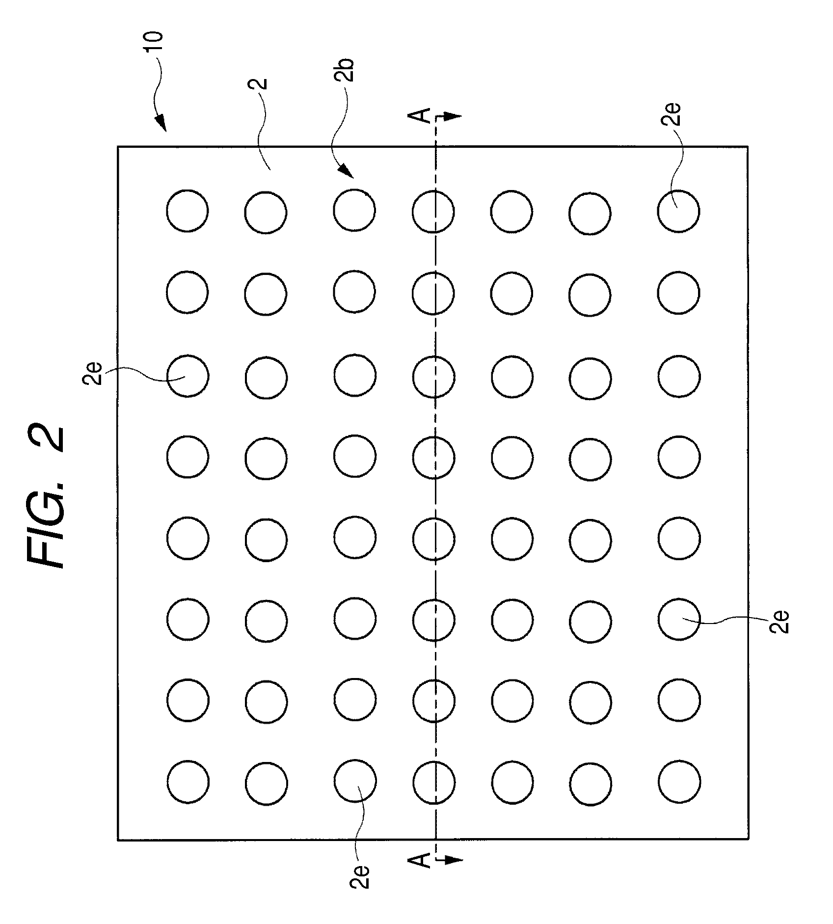
[0142]First, description will be given to the general configuration of a semiconductor device (semiconductor integrated circuit device) 10 in the first embodiment with reference to FIG. 1 to FIG. 3.
[0143]FIG. 1 is a plan view of a wiring substrate (board) mounted with a semiconductor chip in the first embodiment as viewed from the upper surface (front face) side; FIG. 2 is a plan view of the wiring substrate illustrated in FIG. 1 as viewed from the lower surface (rear surface) positioned on the opposite side to the upper surface; and FIG. 3 is a sectional view taken along line A-A of FIG. 1. Over the upper surface of the wiring substrate, as illustrated in FIG. 3, an encapsulating body (resin encapsulating body) for encapsulating the semiconductor chip is formed. In FIG. 1, this encapsulating body is intentionally omitted so that the internal configuration is understandable. In the following plan views illustrating a wiring substrate mounted with a semiconductor chip as viewed from ...
second embodiment
[0213]The semiconductor device 20 in the second embodiment is configured as illustrated in FIG. 38. That is, the multiple bonding leads 24c of a wiring substrate 24 and the multiple pads 1c of a semiconductor chip 1 are respectively electrically coupled together through multiple bump electrodes 21 as conductive members. The bonding leads and the pads are electrically coupled together so that the main surface 1a of the semiconductor chip 1 is opposed to the upper surface 2a of the wiring substrate 24.
[0214]Hereafter, description will be given to features of the semiconductor device 20 in the second embodiment. However, with respect to the same configuration, effect, and the like as in the first embodiment, the description thereof will be omitted.
[0215]FIG. 36 is a plan view of a wiring substrate (board) mounted with a semiconductor chip as viewed from the upper surface (front face, first face) side; FIG. 37 is a plan view of the wiring substrate as viewed from the lower surface (rear...
third embodiment
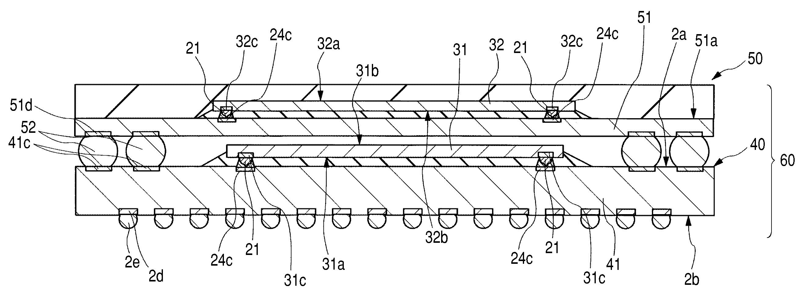
[0235]In the description of the first and second embodiments, semiconductor devices 10, 20 with one semiconductor chip 1 mounted over the upper surface 2a of a wiring substrate 2, 24 have been taken as examples. In conjunction with the enhancement of functionality of semiconductor devices, SIP (System In Package) type semiconductor devices have been discussed in recent years. In the SIP type semiconductor device, a microcomputer semiconductor chip (microcomputer chip) having a computation circuit and a memory semiconductor chip (memory chip) having a memory circuit are mounted together in one semiconductor device to build one system.
[0236]Consequently, the present inventors examined such a SIP type semiconductor device.
[0237]Before the configuration of the semiconductor device 30 in the third embodiment is described, description will be given to the circuit operation of the SIP type semiconductor device in the third embodiment with reference to the circuit block diagram in FIG. 41. ...
PUM
 Abstract
Description
Claims
Application Information