Transient emission scanning microscopy

a scanning microscopy and emission technology, applied in the direction of electronic circuit testing, measurement devices, instruments, etc., can solve the problems of high-precision mechanical stages with sub-micron positioning accuracy, inability to address targets, and inability to align the laser imaging portion of the microscop

Inactive Publication Date: 2009-12-03
QUANTUM FOCUS INSTR CORP
View PDF4 Cites 17 Cited by
  • Summary
  • Abstract
  • Description
  • Claims
  • Application Information

AI Technical Summary

Benefits of technology

[0011]The present invention provides an apparatus for analyzing an integrated circuit to which one or more test signals are applied. An example apparatus includes an objective lens that views reflections from the integrated circuit, a device that houses at least two optical fibers, a component that receives reflections from the objective lens and directs the received reflections to different ones of the at least two optical fibers, and a photo-diode that receives a reflection received by one of at least two optical fibers and adapted to detect a photoemission from the integrated circuit.

Problems solved by technology

Specifically, the issue of how to co-align the laser imaging portion of the microscope with the photon-emission portion of the microscope needed to point at the target is not addressed.
For a single point detector and the scale size of current integrated circuits; expensive, high-precision mechanical stages with sub-micron positioning accuracy are required to achieve the required pointing.

Method used


Image

  • Transient emission scanning microscopy
  • Transient emission scanning microscopy
  • Transient emission scanning microscopy

Examples


Embodiment Construction

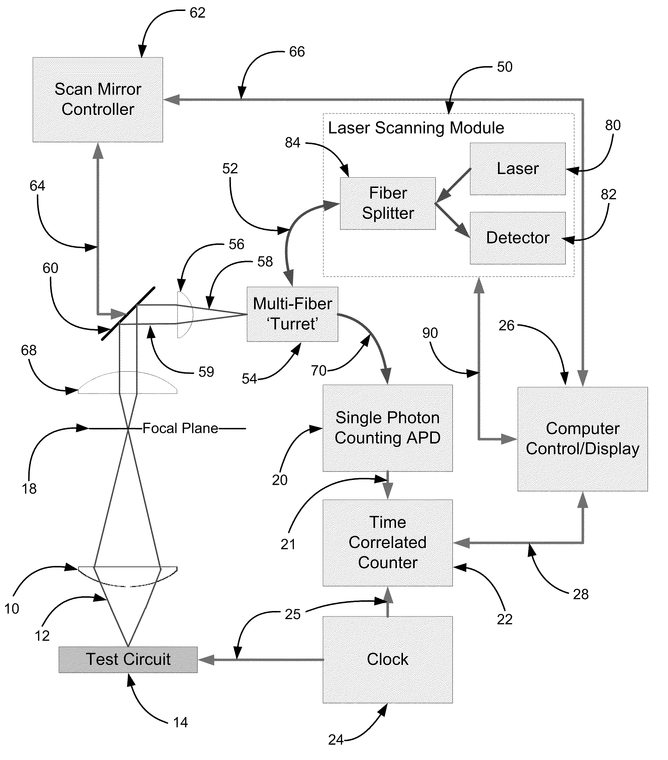
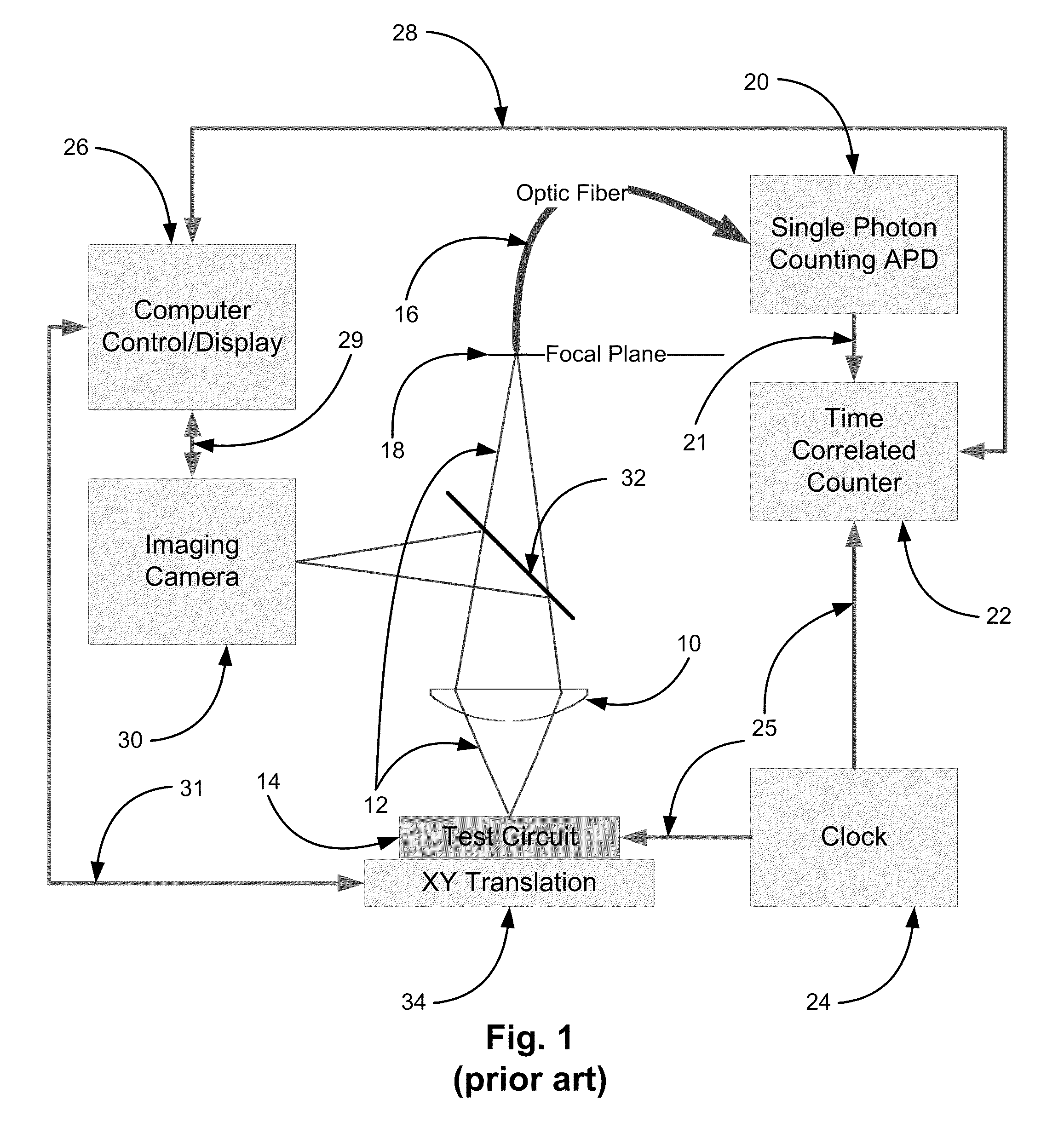
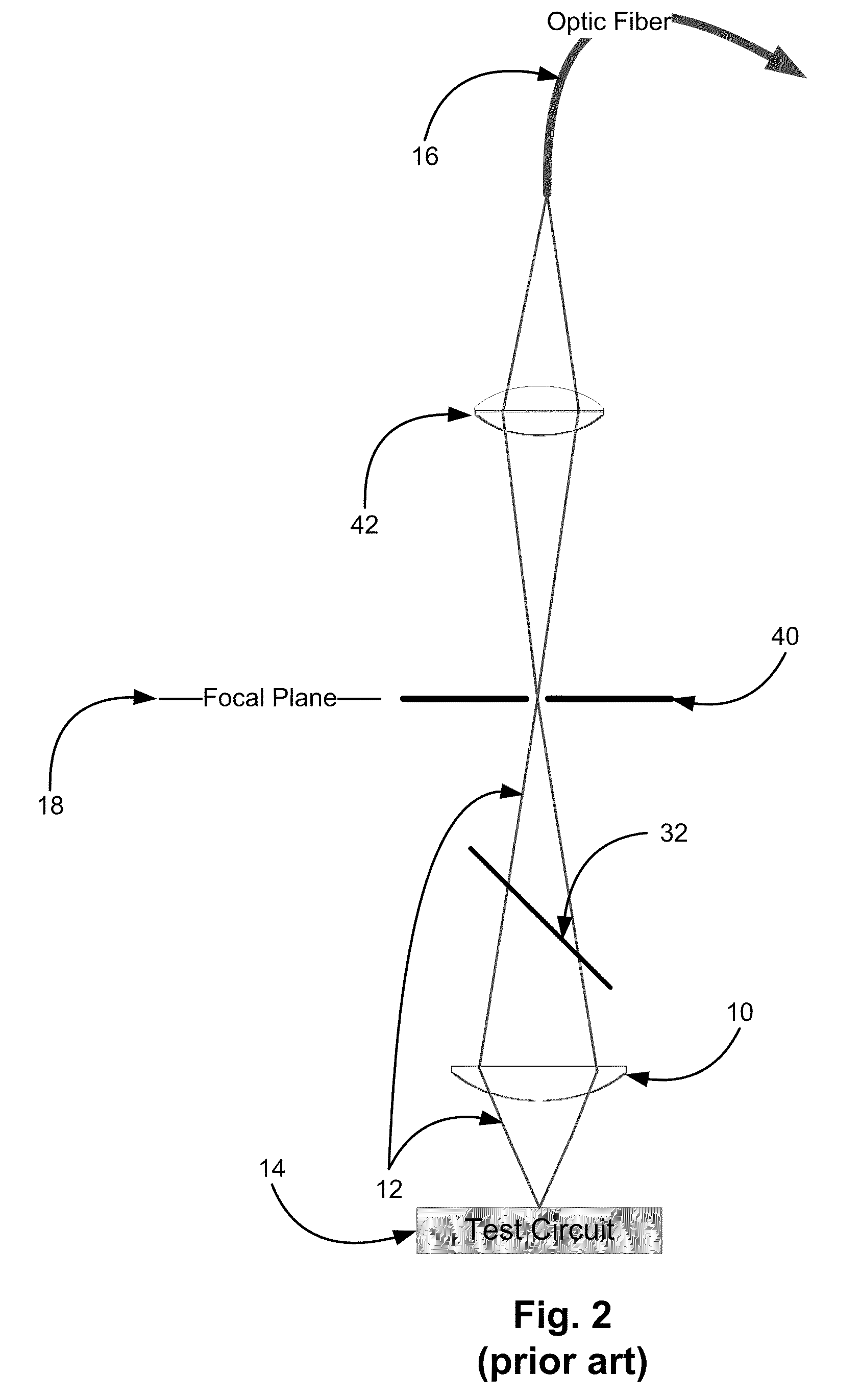
[0014]The prior art is first described in order to better clarify the differences with the current invention. FIG. 1 shows the basic components of a single-point transient-emission detection system as described in the first configuration of U.S. Pat. No. 5,940,545 and in U.S. Pat. No. 6,608,494. A microscope objective 10 focuses optical emission 12 from a test circuit 14 onto the end of an optical fiber 16 at the objective focal plane 18. The optical fiber 16 couples into a single photon counting detector 20 (e.g. an Avalanche Photodiode (APD)). Although the detector 20 could be placed directly into the focal plane 18, the use of an optical fiber 16 as fiber coupling adds flexibility to the design. Photons arriving at the detector 20 create an electrical pulse which is electrically connected 21 to a time correlated counter 22. The time correlated counter 22 records the pulse arrival time. The collection of several pulses allows the counter 22 to produce a histogram of the arrival ti...


PUM


Abstract

An apparatus for analyzing an integrated circuit to which one or more test signals are applied. An example apparatus includes an objective lens that views reflections from the integrated circuit, a device that houses at least two optical fibers, a component that receives reflections from the objective lens and directs the received reflections to the device, and a photo-diode that receives a reflection received by the device. The apparatus includes a beam splitter that directs reflections from the integrated circuit to a detector. A processing device generates an image signal based on a signal received from the detector and a display outputs an image based on the image signal. The component includes a scan mirror that reflects the collimated reflections to a collimating lens that focuses the reflections from the scan mirror toward the device.

Description

PRIORITY CLAIM[0001]This application claims the benefit of U.S. Provisional Application Ser. No. 61 / 058,171 filed Jun. 2, 2008, the contents of which are hereby incorporated by reference.FIELD OF THE INVENTION[0002]This invention is directed towards detection of transient emissions from semiconductor devices.BACKGROUND OF THE INVENTION[0003]U.S. Pat. No. 5,940,545 by Kash and Tsang describes the use of photon timing detection to determine the switching time of transistors in a semiconductor integrated circuit. Kash et al. describe how typical digital circuits will only emit photons during the switching transient. These photons are detected and the arrival time is recorded. Two techniques are described. Both techniques utilize a time-to-amplitude converter and a multi-channel analyzer to determine the photon arrival time and sort the collected data into a time histogram. The first technique utilizes a single avalanche photodiode with a fiber optic probe placed over the sampling area ...

Claims


Application Information

Patent Timeline
Patent Type & Authority Applications(United States)
IPC IPC(8): G01R31/302G01R31/02
CPCG01R31/311
Inventor FALK, R. AARON
Owner QUANTUM FOCUS INSTR CORP
Why Eureka
Try Eureka