Compensation scheme for multi-color electroluminescent display

a multi-color electroluminescent display and compensation scheme technology, applied in the direction of electrical testing, measurement devices, instruments, etc., can solve the problems of reducing the lifetime of the display, reducing the dynamic range and image artifacts, and reducing the efficiency of the display, so as to achieve the effect of simple voltage measurement circuitry

Active Publication Date: 2009-12-03
GLOBAL OLED TECH
View PDF20 Cites 65 Cited by
  • Summary
  • Abstract
  • Description
  • Claims
  • Application Information

AI Technical Summary

Benefits of technology

[0013]It is therefore an object of the present invention to compensate for aging and efficiency changes in electroluminescent emitters in the presence of transistor aging.
[0025]An advantage of this invention is an electroluminescent (EL) display that compensates for the aging of the organic materials in the display wherein circuitry aging is also occurring, without requiring extensive or complex circuitry for accumulating a continuous measurement of light-emitting element use or time of operation. It is a further advantage of this invention that it uses simple voltage measurement circuitry. It is a further advantage of this invention that by making all measurements of voltage, it is more sensitive to changes than methods that measure current. It is a further advantage of this invention that it performs the compensation based separately on EL changes and changes in driving transistor properties. It is a further advantage of this invention that compensation for changes in driving transistor properties can be performed with compensation for the EL changes, thus providing a complete compensation solution. It is a further advantage of this invention that both aspects of measurement and compensation (EL and driving transistor) can be accomplished rapidly. It is a further advantage of this invention that characterization and compensation of driving transistor and EL changes are unique to the specific element and are not impacted by other elements that can be open-circuited or short-circuited.

Problems solved by technology

This Vth shift can result in decreased dynamic range and image artifacts.
Moreover, the organic materials in OLED and hybrid EL devices also deteriorate in relation to the integrated current density passed through them over time, so that their efficiency drops while their resistance to current, and thus forward voltage, increases.
These two factors, TFT and EL aging, reduce the lifetime of the display.
Different organic materials on a display can age at different rates, causing differential color aging and a display whose white point varies as the display is used.
If some EL devices in the display are used more than others, spatially differentiated aging can result, causing portions of the display to be dimmer than other portions when driven with a similar signal.
This can result in visible burn-in.
Differences in signal format are also problematic.
Furthermore, the matte areas are not aged as quickly as the image area in these cases, which can result in the matte areas' being objectionably brighter than the 16:9 image area when a 4:3 (full-screen) image is displayed.
However, such circuits are typically much larger and more complex than the two-transistor, single capacitor (2T1C) circuits otherwise employed, thereby reducing the aperture ratio (AR), the percent of the area on a display available for emitting light.
These additional signal lines reduce aperture ratio and add assembly cost.
This doubles the number of lines that have to be bonded to driver integrated circuits, increasing the cost of an assembled display, and increasing the probability of bond failure, thus decreasing the yield of good displays from the assembly line.
This problem is particularly acute for large-format, high-resolution displays, which can have over two thousand columns.
However, it also affects smaller displays, as higher bondout counts can require higher-density connections, which are more expensive to manufacture and have lower yield than lower-density connections.
This solution is unlikely to be acceptable to most viewers because of the cost and inconvenience.
As indicated therein, however, such estimation is not perfect, resulting in a reduced, but still present, non-uniform aging.
However, these solutions can cause objectionable image artifacts, for example reduced sharpness or visibly brighter border areas in displayed images.
This method requires the detection of static areas and cannot prevent color-differentiated burn-in.
However, this approach requires a prior knowledge and control of the image signal and does not address the problem of format differences.
However, these techniques cannot employ all pixels of a display, and therefore can create a border effect of pixels that are brighter than those pixels in the image area that are always used to display image data.
Methods requiring additional display circuitry can reduce the lifetime of the display, increase its cost, and reduce manufacturing yield.
Methods manipulating the displayed image cannot correct for all burn-in.

Method used


Image

  • Compensation scheme for multi-color electroluminescent display
  • Compensation scheme for multi-color electroluminescent display
  • Compensation scheme for multi-color electroluminescent display

Examples


Embodiment Construction

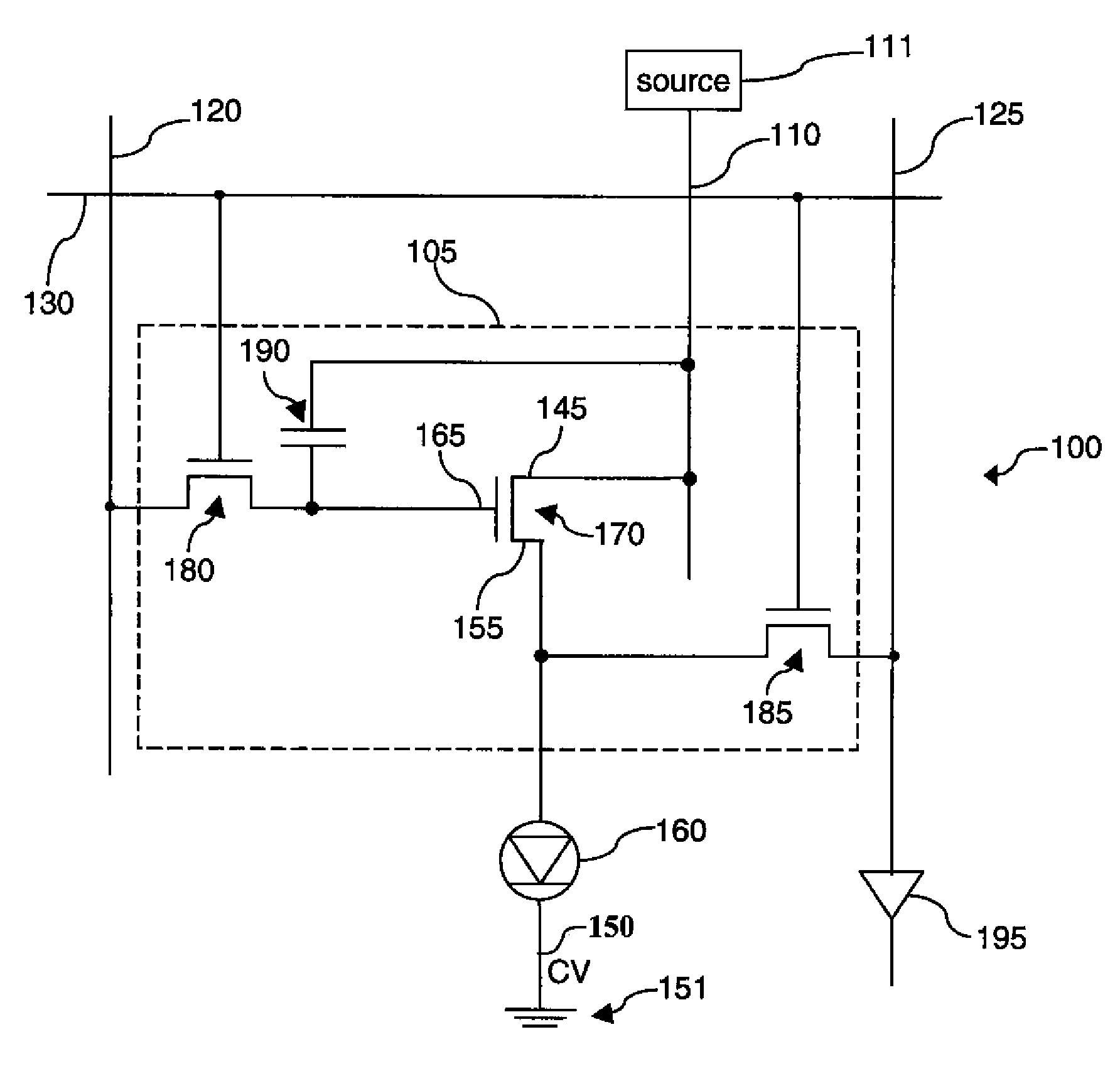
[0031]Turning now to FIG. 1, there is shown a schematic diagram of an electroluminescent (EL) pixel as described by Levey et al. in above-cited commonly assigned U.S. patent application Ser. No. 11 / 766,823. Such pixels are well known in the art in active matrix EL displays. One useful example of an EL display is an organic light-emitting diode (OLED) display. EL pixel 100 includes a light-emitting EL device 160 and a drive circuit 105. EL pixel 100 is connected to a data line 120, a first power supply line 110 driven by a first voltage source 111, a select line 130, and a second power supply line 150 driven by a second voltage source 151. By “connected” or “electrically connected” it is meant that the elements are directly connected or connected via another component, e.g. a switch, a diode, another transistor, etc. Drive circuit 105 includes a drive transistor 170, a switch transistor 180, and a capacitor 190. Drive transistor 170 can be an amorphous-silicon (a-Si) thin-film transi...


PUM


Abstract

A method of determining characteristics of transistors and electroluminescent devices, includes: providing an electroluminescent display; providing for pairs of electroluminescent devices drive circuits and a single readout line, each drive circuit including a readout transistor electrically connected to the readout line; providing a first voltage source; providing a second voltage source; providing a current source; providing a current sink; providing a test voltage source; providing a voltage measurement circuit; sequentially testing the drive transistors to provide a first signal representative of characteristics of the drive transistor of the first drive circuit and a second signal representative of characteristics of the drive transistor of the second drive circuit, whereby the characteristics of each drive transistor are determined; and simultaneously testing the first and second electroluminescent devices to provide a third signal representative of characteristics of the pair of electroluminescent devices, whereby the characteristics of both electroluminescent devices are determined.

Description

CROSS REFERENCE TO RELATED APPLICATIONS[0001]Reference is made to commonly assigned U.S. patent application Ser. No. 11 / 766,823 filed Jun. 22, 2007, entitled “OLED Display with Aging and Efficiency Compensation” by Levey et al.; U.S. patent application Ser. No. 11 / 946,392 filed Nov. 28, 2007, entitled “Electroluminescent Display with Interleaved 3T1C” by White et al.; and U.S. patent application Ser. No. ______ filed concurrently herewith entitled “Compensation Scheme for Multi-Color Electroluminescent Display” by Levey et al the disclosures of which are incorporated herein by reference.FIELD OF THE INVENTION[0002]The present invention relates to solid-state electroluminescent flat-panel displays and more particularly to such displays having ways to compensate for the aging of the organic light emitting display components.BACKGROUND OF THE INVENTION[0003]Electroluminescent (EL) devices are a promising technology for flat-panel displays. For example, Organic Light Emitting Diodes (OL...

Claims


Application Information

Patent Timeline
Patent Type & Authority Applications(United States)
IPC IPC(8): G01R31/26
CPCG09G3/006G09G3/3233G09G2300/0866G09G2300/0439G09G3/325
Inventor LEVEY, CHARLES I.
Owner GLOBAL OLED TECH
Why Eureka
Try Eureka