Method for manufacturing Chalcogenide devices

Inactive Publication Date: 2009-12-03
OVONYX
View PDF7 Cites 43 Cited by
  • Summary
  • Abstract
  • Description
  • Claims
  • Application Information

AI Technical Summary

Benefits of technology

[0016]In accordance with the principles of the present invention, the surface upon which the chalcogenide material is deposited may be treated using any of a variety of processes, including dilute hydrogen fluoride bath, degassing, soft sputter etching, densification, and reactive plasma cleaning, or combinations thereof. Such pre-deposition treatment reduces or eliminates native oxides and other contaminants from the surface, thereby increasing the adhesion of the chalcogenide layer to the treated surface. Voids between the chalcogenide layer and deposition surface are substantially eliminate

Problems solved by technology

Because different types of chalcogenide material may be deposited upon different types of surface materials, using different features (e.g., a pore within the deposition surface) with various topolo

Method used


Image

  • Method for manufacturing Chalcogenide devices
  • Method for manufacturing Chalcogenide devices

Examples


Embodiment Construction

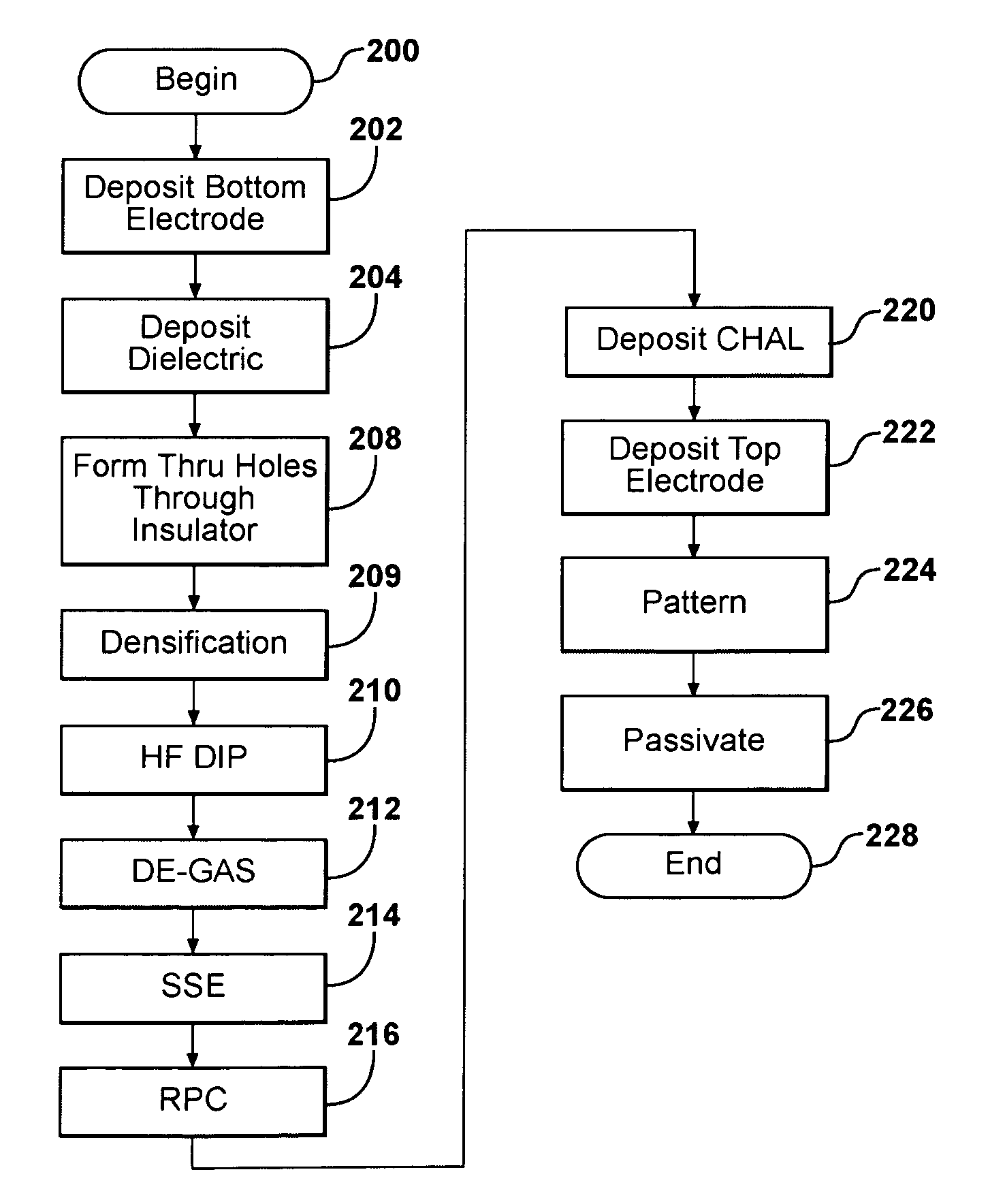
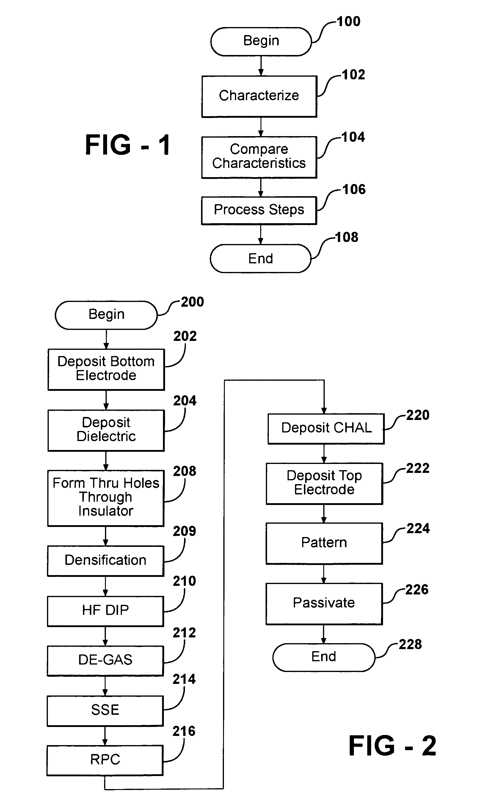
[0021]Although this invention will be described in terms of certain preferred embodiments, other embodiments that are apparent to those of ordinary skill in the art, including embodiments that do not provide all of the benefits and features set forth herein, are also within the scope of this invention. Various structural, logical, process step, and electrical changes may be made without departing from the spirit or scope of the invention.

[0022]The term “substrate” used in the following description may include any supporting structure including, but not limited to, a semiconductor substrate that has an exposed electrically conducting surface. The term semiconductor substrate may include, for example, silicon on insulator (SOI), silicon on sapphire (SOS), doped and undoped semiconductors, epitaxial layers of silicon supported by a base semiconductor foundation, and other semiconductor structures. When reference is made to substrate, semiconductor substrate, or wafer in the following d...


PUM


Abstract

A method of chalcogenide device formation includes treatment of the surface upon which the chalcogenide material is deposited. The treatment reduces or eliminates native oxides and other contaminants from the surface, thereby increasing the adhesion of the chalcogenide layer to the treated surface, eliminating voids between the chalcogenide layer and deposition surface and reducing the degradation of chalcogenide material due to the migration of contaminants into the chalcogenide.

Description

CROSS-REFERENCE TO RELATED APPLICATIONSFIELD OF INVENTION[0001]This invention pertains to phase change electronic devices, and, more particularly, to methods of producing phase change electronic devices that exhibit desirable resistance characteristics.BACKGROUND OF THE INVENTION[0002]Phase-change electronic devices include memory devices, referred to herein as Ovonic Universal Memory (OUM), and switching devices, referred to herein as Ovonic Threshold Switches (OTS). OUM cells utilize a class of materials that are reversibly switchable from one material phase to another with measurable distinct electrical properties associated with each phase. For example, these materials may change between an amorphous disordered phase and a crystalline, or polycrystalline, ordered phase, with a significant corresponding change in the thermal and electrical conductivity of the material. Chalcogenide materials are typically employed as the phase change material used in both OUM and OTS cells. A wid...

Claims


Application Information

Patent Timeline
IPC IPC(8): H01L45/00
CPCH01L45/04H01L45/1608H01L45/144H01L45/06H10N70/20H10N70/231H10N70/021H10N70/8828
Inventor LOWREY, TYLERFOURNIER, JEFFNUSS, ROBERTSCHELL, CARLWICKER, GUYRICKER, JIMREED, JAMESSPALL, EDKOSTYLEV, SERGEYCZUBATYJ, WOLODYMYRSANDOVAL, REGINO
Owner OVONYX
Why Eureka
Try Eureka