Self-aligned in-contact phase change memory device

a phase change memory and self-aligning technology, applied in the field of computer memory, can solve the problem that the change material does not utilize chalcogen

Inactive Publication Date: 2009-12-03
GLOBALFOUNDRIES US INC
View PDF2 Cites 52 Cited by
  • Summary
  • Abstract
  • Description
  • Claims
  • Application Information

AI Technical Summary

Problems solved by technology

However, some phase change materials do not utilize chalcogen, such as GeSb.

Method used


Image

  • Self-aligned in-contact phase change memory device
  • Self-aligned in-contact phase change memory device
  • Self-aligned in-contact phase change memory device

Examples


Embodiment Construction

[0018]The present invention will be described with reference to embodiments of the invention. Throughout the description of the invention reference is made to FIGS. 1-9. When referring to the figures, like structures and elements shown throughout are indicated with like reference numerals.

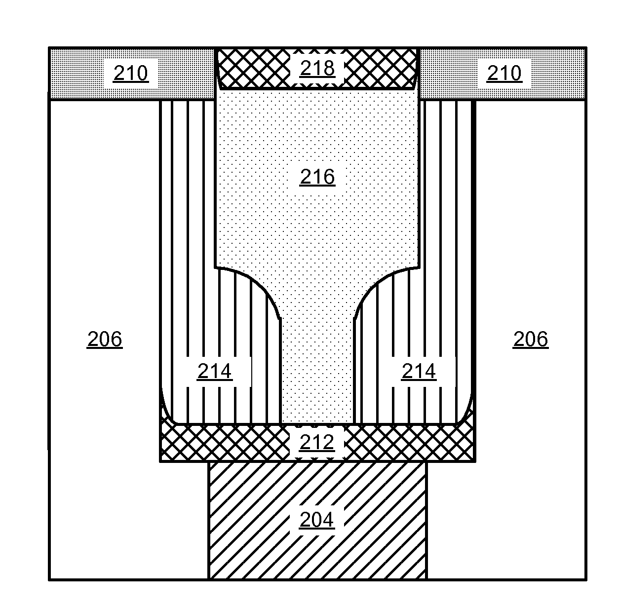
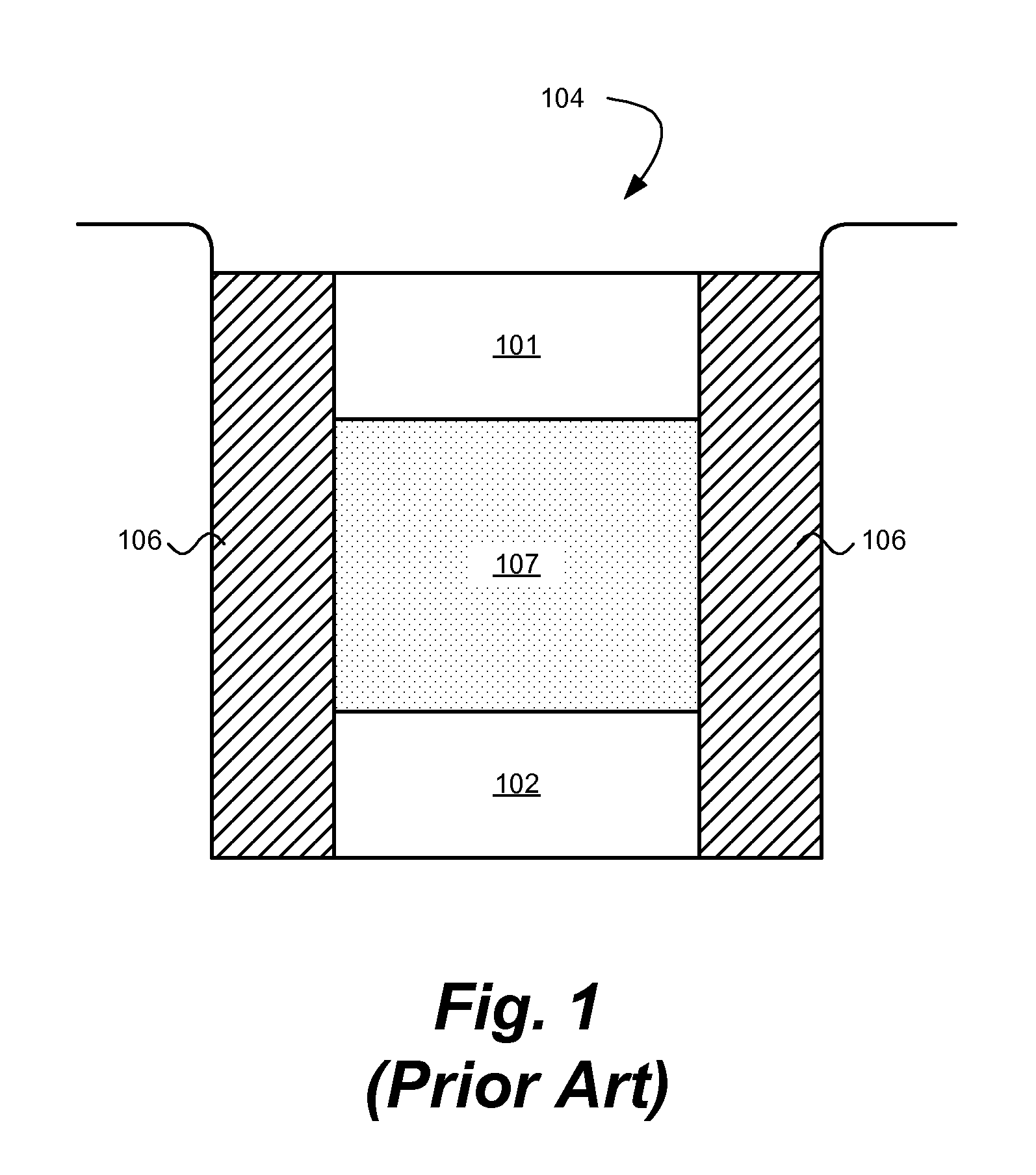
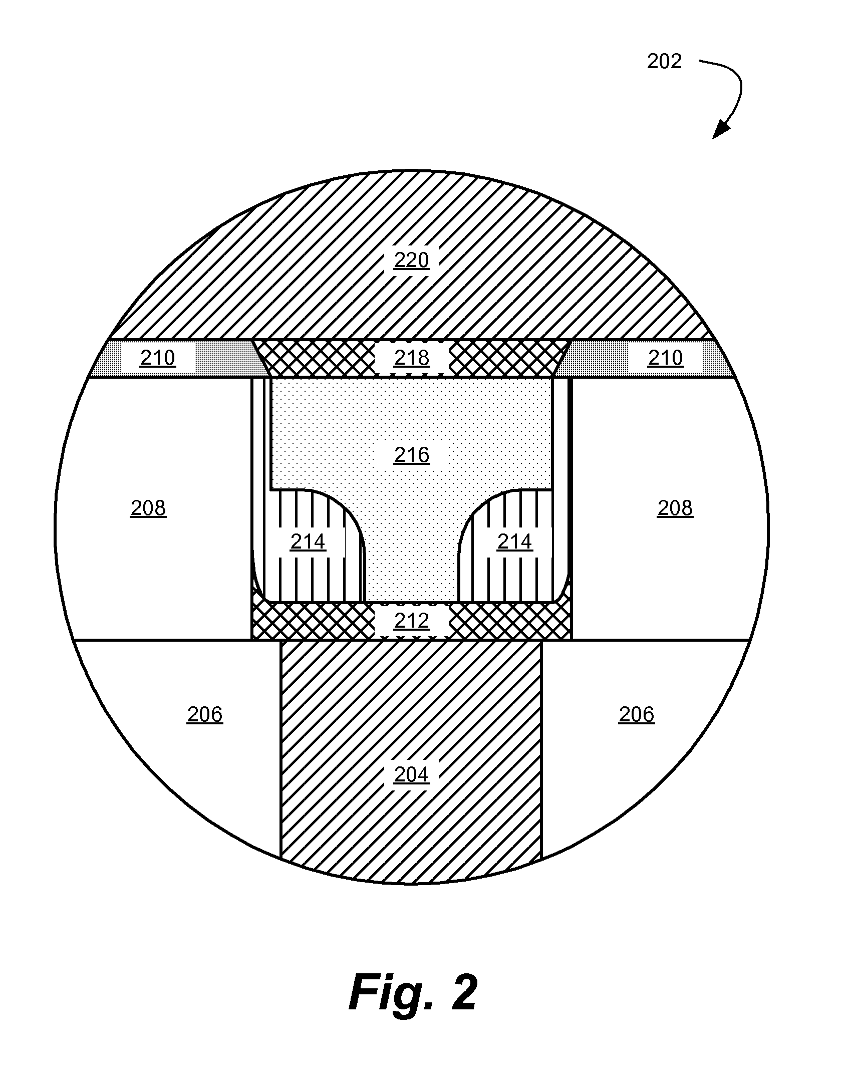
[0019]FIG. 2 illustrates a cross sectional view of an exemplary memory cell 202 contemplated by the present invention. The memory cell 202 includes a conductive lower block 204 in a via in at least one layer of insulating material 206, 208 and 210, a heat-isolating conductive lower layer 212 above the conductive lower block 204, an insulating step spacer 214 above the heat-isolating conductive lower layer 212, phase change material 216 disposed above the heat-isolating conductive lower layer 212 and within the step spacer 214, a heat-isolating conductive upper layer 218, and a conductive upper block 220. The cell 202 is typically formed on a substrate with metal-oxide-semiconductor field-effect tra...


PUM


Abstract

A memory cell and a method of making the same, that includes insulating material deposited on a substrate, a bottom electrode formed within the insulating material, a plurality of insulating layers deposited above the bottom electrode and at least one of which acts as an intermediate insulating layer. Then defining a via in the insulating layers above the intermediate insulating layer, creating a channel for etch with a step spacer, defining a pore in the intermediate insulating layer, removing all insulating layers above the intermediate insulating layer, filling the entirety of the pore with phase change material, and forming an upper electrode above the phase change material. Additionally, the formation of bit line connections with the upper electrode.

Description

CROSS-REFERENCE TO RELATED APPLICATIONS[0001]This application is a divisional application claiming priority under 35 U.S.C. § 120 to U.S. patent application Ser. No. 11 / 550,318 filed Oct. 17, 2006, the entire text of which is specifically incorporated by reference herein.FIELD OF THE INVENTION[0002]The present invention is directed toward computer memory, and more particularly to a non-volatile phase change memory device.BACKGROUND OF THE INVENTION[0003]There are two major groups in computer memory: non-volatile memory and volatile memory. Constant input of energy in order to retain information is not necessary in non-volatile memory but is required in the volatile memory. Examples of non-volatile memory devices are Read Only Memory, Flash Electrical Erasable Read Only Memory, Ferroelectric Random Access Memory, Magnetic Random Access Memory, and Phase Change Memory. Examples of volatile memory devices include Dynamic Random Access Memory (DRAM) and Static Random Access Memory (SRAM...

Claims


Application Information

Patent Timeline
Patent Type & Authority Applications(United States)
IPC IPC(8): H01L47/00H01L21/10
CPCH01L21/76831H01L27/2436H01L45/06H01L45/1683H01L45/144H01L45/148H01L45/1233H10B63/30H10N70/231H10N70/826H10N70/884H10N70/8828H10N70/066
Inventor CHEEK, ROGER W.LAM, CHUNG H.ROSSNAGEL, STEPHEN M.SCHROTT, ALEJANDRO G.
Owner GLOBALFOUNDRIES US INC
Why Eureka
Try Eureka