Liquid crystal display device and method for driving same

a liquid crystal display and display device technology, applied in the direction of instruments, computing, electric digital data processing, etc., can solve the problems of unsuitable application voltage in the range of 2v and above configuration, and achieve the effect of simplifying the power supply circuit, facilitating voltage withstanding design of the driver circuit, and narrowing the drive voltage rang

Inactive Publication Date: 2009-12-10
SHARP KK
View PDF12 Cites 20 Cited by
  • Summary
  • Abstract
  • Description
  • Claims
  • Application Information

AI Technical Summary

Benefits of technology

[0043]According to the first aspect of the present invention, with the configuration in which the auxiliary capacitance lines are driven such that the third or fourth potential is applied at or after the first time point so as to be changed in the same direction as the direction in which the potential of the common electrode is changed at the first time point, and the applied potential is maintained for a predetermined period until the second time point or a time point before and close to the second time point, it is possible to keep the range of drive voltage narrow, thereby facilitating voltage withstanding design for driver circuits, while increasing the difference between the maximum and minimum absolute values of voltage to be applied to the liquid crystal by taking advantage of dielectric anisotropy of the liquid crystal with respect to the applied voltage.
[0044]According to the second aspect of the present invention, at least two of the fifth potential, the first potential, and the third potential are approximately equal, which eliminates the need to generate a wide variety of potentials in the power supply circuit, making it possible to simplify the power supply circuit.
[0045]According to the third aspect of the present invention, at leas

Problems solved by technology

Therefore, without any modification, the above configuration is not appropriate because the voltage applied to the liquid crystal varies in the range of ±2V.
Note that in the case of normally white TN mode liquid cryst

Method used


Image

  • Liquid crystal display device and method for driving same
  • Liquid crystal display device and method for driving same
  • Liquid crystal display device and method for driving same

Examples


Embodiment Construction

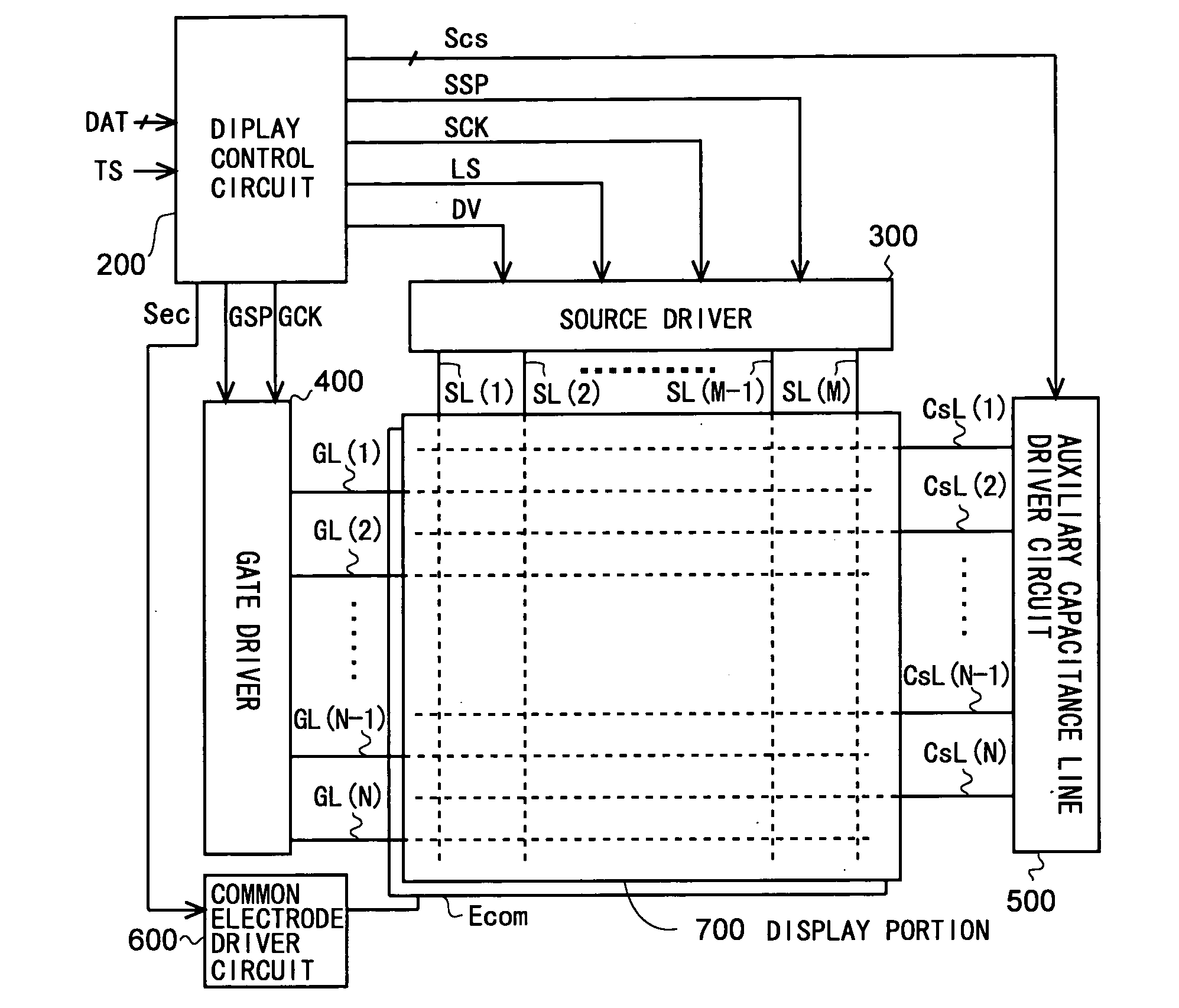
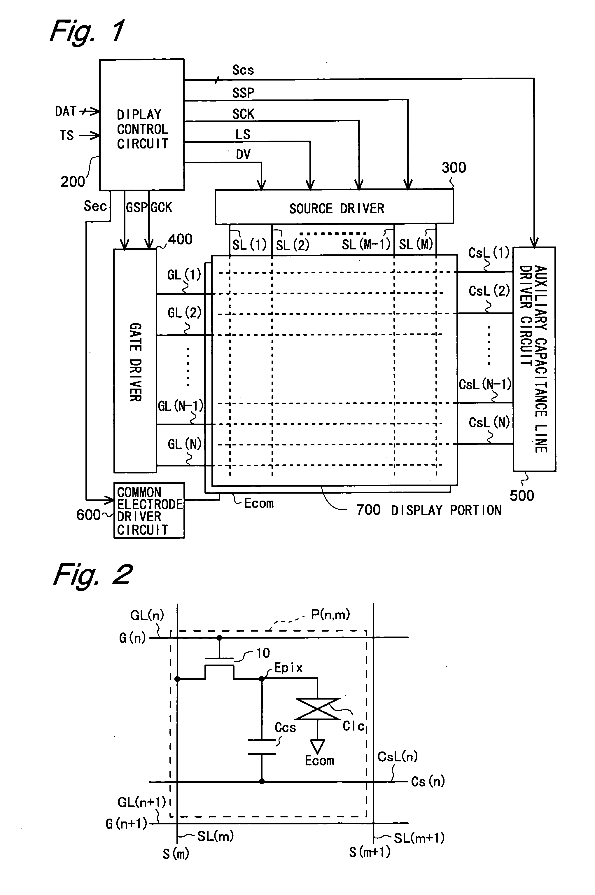
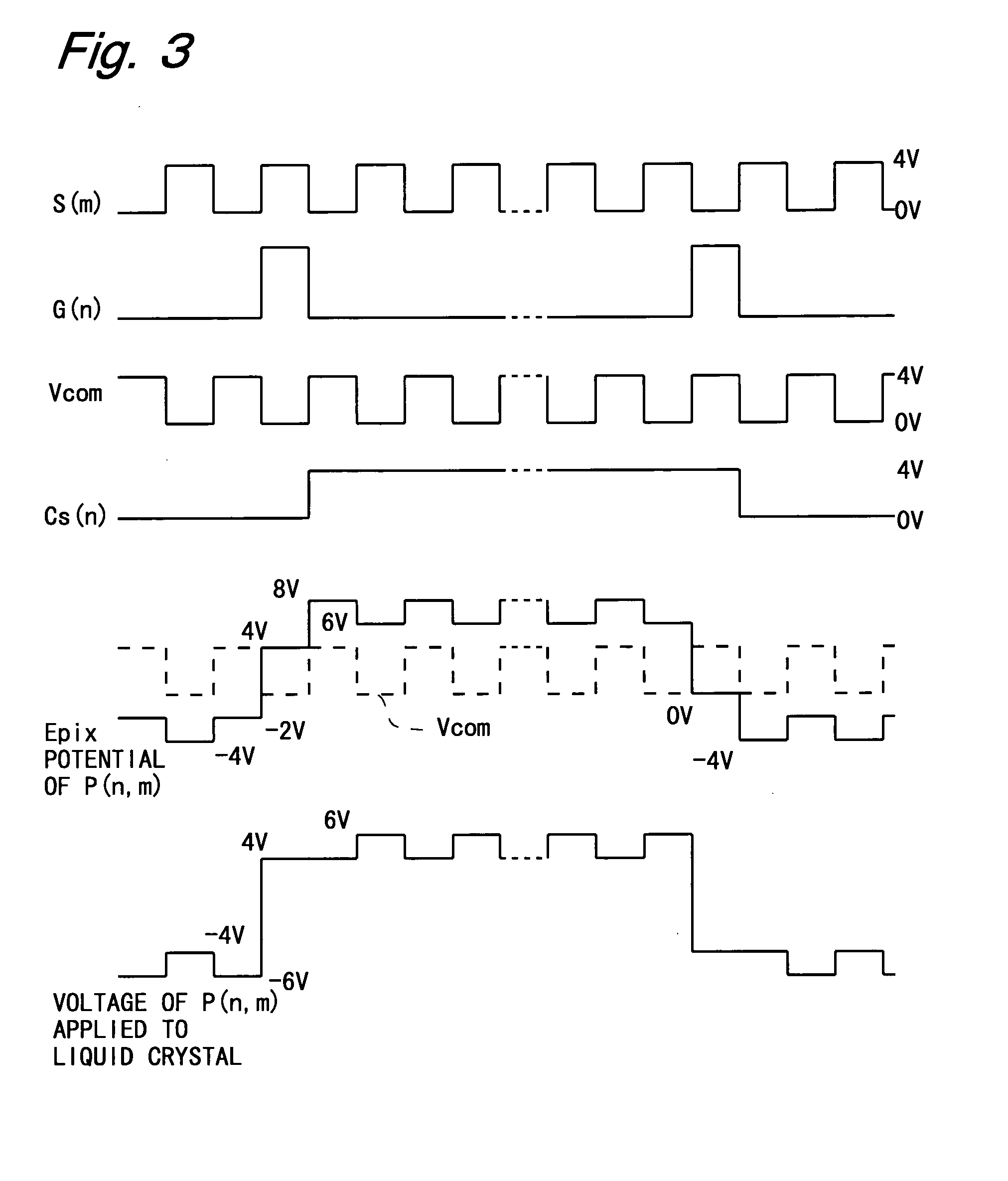
[0074]Hereinafter, embodiments of the present invention will be described with reference to the accompanying drawings. In the following description, the display portion is configured in a vertically-aligned, normally-black mode, and employs a so-called line-inversion drive method, which is a drive method in which voltage applied to the liquid crystal part of the pixel formation portion is inverted in polarity between adjacent rows and also frame by frame. Note that a so-called n-line inversion drive method may be employed in which the polarity is inverted every two rows or more.

[0075]

[0076]FIG. 1 is a block diagram illustrating the overall configuration of an active-matrix liquid crystal display device according to an embodiment of the present invention. This liquid crystal display device includes a drive control portion and a display portion 700, the drive control portion consisting of a display control circuit 200, a source driver (video signal line driver circuit) 300, a gate dri...


PUM


Abstract

One embodiment of the present invention provides a liquid crystal display device in which auxiliary capacitance lines are driven, thereby allowing the range of drive voltage to be kept narrow while increasing the difference between the maximum and minimum absolute values of voltage to be applied to liquid crystal, and in the present liquid crystal display device, the voltage ranges for an auxiliary capacitance line drive signal, a video signal, and a common potential are equally maintained as low as from 0V to 4V, while inverting the common potential every scanning period and causing the potential of the auxiliary capacitance line drive signal to rise in the same direction as the common potential at the time of the fall of the scanning signal such that the potential is maintained until the next frame. With this configuration, it is possible to set the maximum absolute value of the voltage applied to the liquid crystal at about 5V, which corresponds to an effective value of the applied voltage, while setting the minimum value at about 1.5V, which is also an effective value of the applied voltage, thereby increasing the difference between the maximum and minimum values.

Description

TECHNICAL FIELD[0001]The present invention relates to active-matrix liquid crystal display devices using switching elements, such as thin-film transistors, and methods for driving the same, more particularly to a liquid crystal display device and a drive method thereof, in which auxiliary capacitance lines are driven by changing voltage applied thereto.BACKGROUND ART[0002]In general, a conventional active-matrix liquid crystal display device includes a display portion provided with a plurality (N) of scanning signal lines GL(1) to GL(N), a plurality (M) of video signal lines SL(1) to SL(M) crossing the scanning signal lines, and a plurality (M×N) of pixel formation portions P(1,1) to P(N,M) arranged in a matrix in accordance with intersections of the scanning signal lines and the video signal lines, each pixel formation portion including a liquid crystal capacitance (also referred to as a “pixel capacitance”) Clc formed by a pixel electrode and an electrode (also referred to as a “c...

Claims


Application Information

Patent Timeline
IPC IPC(8): G09G3/36
CPCG02F1/136213G09G2330/021G09G2300/0876G09G3/3655
Inventor NAGATA, HISASHI
Owner SHARP KK
Why Eureka
Try Eureka