Display apparatus

a technology for display devices and display devices, applied in the direction of discharge tubes/lamp details, discharge tubes luminescnet screens, electric discharge lamps, etc., can solve the problems of non-display devices, organic light emitting devices, and non-display devices formed outside, etc., to achieve the effect of suppressing deterioration

Active Publication Date: 2009-12-17
CANON KK
View PDF15 Cites 48 Cited by
  • Summary
  • Abstract
  • Description
  • Claims
  • Application Information

AI Technical Summary

Benefits of technology

[0034]In the present invention, the discontinuous part of the planarizing layer serving as the generation source of moisture and a path through which moisture is infiltrated into each organic light emitting device is formed in a nondisplay device provided outside the outermost pixel of the display area. Alternatively, the film formation edge of organic compound layer serving as a path through which moisture is infiltrated into each organic light emitting device is closer to the display area than each nondisplay device, and a pair of electrodes is in contact in each nondisplay device. As a result, the flow of moisture infiltrating into each organic light emitting device through the planarizing layer or the organic compound layer can be shielded. Further, the formation of the discontinuous part of the planarizing layer in each nondisplay device can narrow a nondisplay area (frame), whereby a display apparatus which has a narrow frame and suppresses deterioration owing to moisture can be provided.

Problems solved by technology

In addition, an organic light emitting device deteriorates owing to moisture, so some contrivances to protect the organic light emitting device from external moisture or oxygen are needed.
The organic light emitting device deteriorates owing to the infiltration of not only moisture from the outside but also moisture taken in at the time of the formation of a TFT or of an electrode and present in an area surrounded by the substrate and a sealing film or sealing glass into the organic light emitting device.
However, the nondisplay devices are formed outside the display area, and are not actually driven.

Method used


Image

  • Display apparatus
  • Display apparatus
  • Display apparatus

Examples


first embodiment

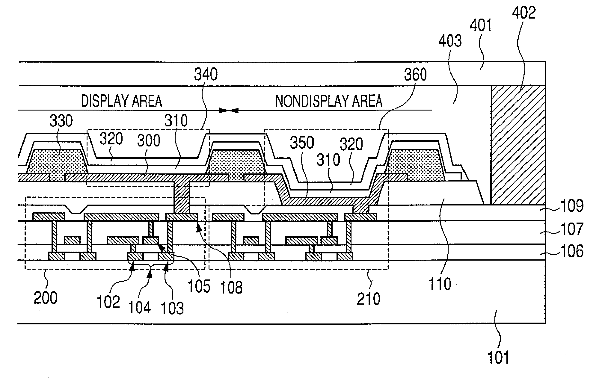
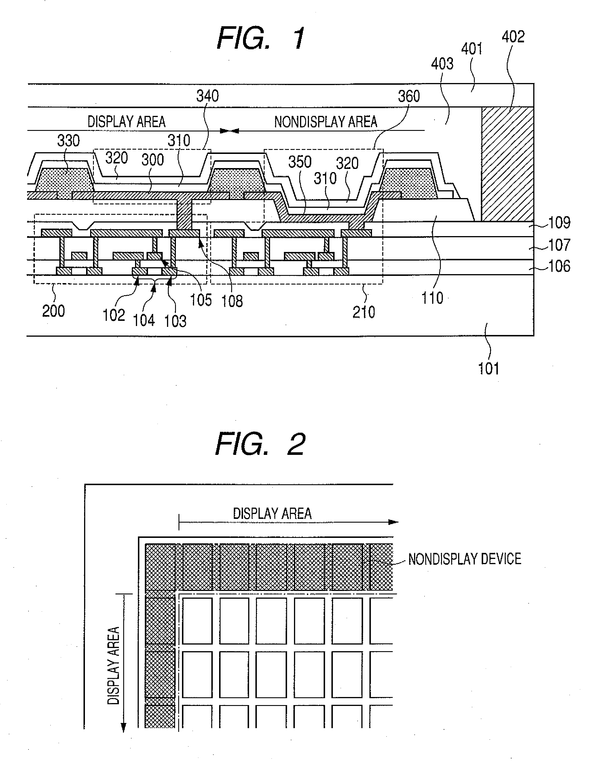
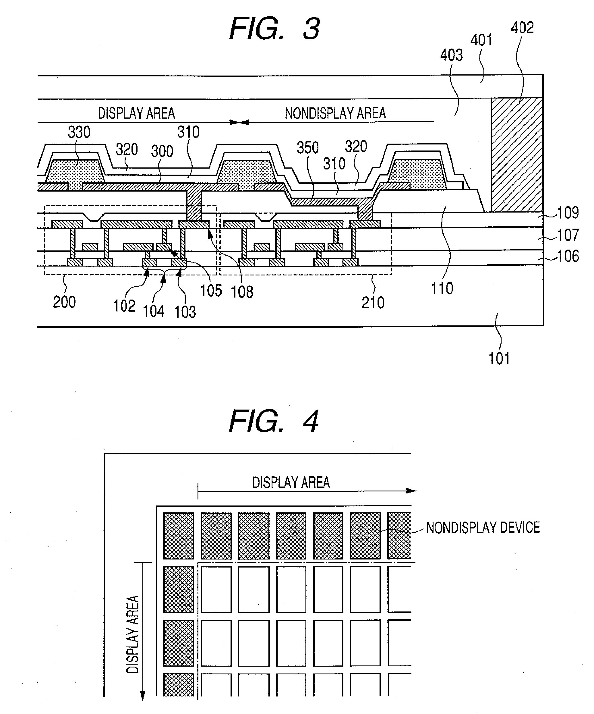
[0047]FIG. 1 is a schematic sectional view showing a display apparatus according to first embodiment of the present invention. In FIG. 1, reference numeral 101 represents a substrate; 102, a source region; 103, a drain region; 104, an active layer; 105, a gate electrode; 106, a gate insulating film; 107, an interlayer insulating film; 108, a drain electrode; 109, an inorganic insulating film; and 110, a planarizing layer. In addition, reference numerals 200 and 210 each represent a thin film transistor (TFT); 300, a first electrode; 310, an organic compound layer; 320, a second electrode; 330, a device isolation film; 340, an organic light emitting device; 350, a third electrode; and 360, a nondisplay device. Reference numeral 401 represents a sealing substrate; 402, an adhesive member; and 403, a gap.

[0048]The display apparatus according to this embodiment has: the substrate 101; the plural TFTs 200 and 201 formed on the substrate; the planarizing layer 110 covering the plural TFTs...

second embodiment

[0073]FIG. 8 is a schematic sectional view showing a display apparatus according to second embodiment of the present invention. Hereinafter, the description of the same constitution as that of first embodiment will be omitted.

[0074]The display apparatus according to this embodiment has: the substrate 101; the plural TFTs 200 and 201 formed on the substrate 101; the planarizing layer 110 covering the plural TFTs; and the plural organic light emitting devices 340 formed on the planarizing layer to form a display area. The display apparatus has the plural nondisplay devices (dummy pixels) 360 formed on the planarizing layer 110 outside the display area.

[0075]Each of the organic light emitting devices 340 has, on the substrate 101, the first electrode 300 patterned for each organic light emitting device, the organic compound layer 310 formed in a continuous manner to straddle organic light emitting devices, and the second electrode in the stated order.

[0076]Each of the nondisplay device...


PUM


Abstract

Provided is a display apparatus including: a substrate; plural thin film transistors formed on the substrate; a planarizing layer covering the plural thin film transistors; plural organic light emitting devices formed on the planarizing layer to form a display area; and plural nondisplay devices formed on the planarizing layer outside the display area. The organic light emitting devices each have a first electrode, an organic compound layer, and a second electrode on the substrate in the stated order. In the display apparatus, in each of the plural nondisplay devices, the discontinuous part of the planarizing layer is formed.

Description

TECHNICAL FIELD[0001]The present invention relates to a display apparatus using an organic EL (an abbreviation of Electro Luminescence, hereinafter abbreviated as “EL”) device, that is, an organic light emitting device.BACKGROUND ART[0002]The development of EL devices each using a thin film formed of a luminous material has been advanced in recent years. In particular, research on, and the development of, an organic EL device have been vigorously advanced because of the potential of the device to serve as a light emitting device having high-speed responsiveness and high efficiency. In general, an organic EL device, that is, an organic light emitting device has such a structure that an anode and a cathode are formed as a pair of electrodes on a substrate, and plural organic compound layers including a light emitting layer are laminated between the pair of electrodes by employing, for example, a vapor deposition method.[0003]A hole transporting layer and a hole injecting layer on an a...

Claims


Application Information

Patent Timeline
Patent Type & Authority Applications(United States)
IPC IPC(8): H01L27/32
CPCH01L27/3244H01L51/5237H01L27/3246H10K59/122H10K59/124H10K59/131H10K50/841H10K59/12
Inventor TAKATA, KENJIMIMURA, TOSHIHIKO
Owner CANON KK
Why Eureka
Try Eureka