Metallization method for solar cells

Active Publication Date: 2009-12-17
SOLARWORLD IND GMBH
View PDF6 Cites 5 Cited by
  • Summary
  • Abstract
  • Description
  • Claims
  • Application Information

AI Technical Summary

Benefits of technology

[0005]It is therefore the object of the invention to provide a method which facilitates the p

Problems solved by technology

This reduces the number of process steps required to prod

Method used


Image

  • Metallization method for solar cells
  • Metallization method for solar cells
  • Metallization method for solar cells

Examples


Example

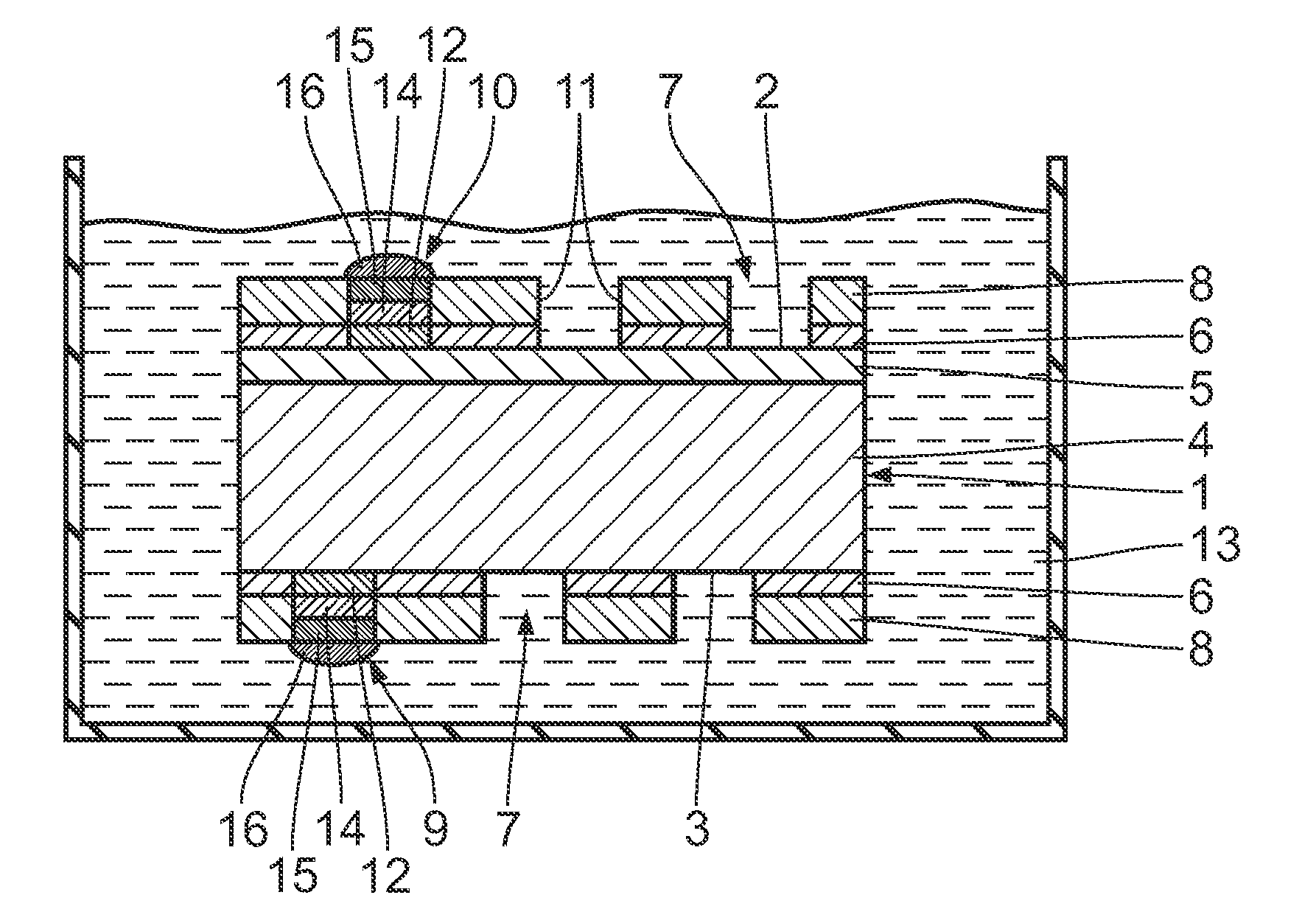
[0016]The following is a description of a first embodiment of the invention with reference to FIG. 1. In a first step, a flat—in other words two-dimensional—semiconductor substrate 1 having a front side 2 and a back side 3 is doped with a dopant by means of processes known to those skilled in the art. After doping, the semiconductor substrate 1 comprises at least one p-doped region 4 and at least one n-doped region 5. According to the first embodiment of the invention, both the p-doped region 4 and the n-doped region 5 are simply connected. The p-doped region 4 and the n-doped region 5 are arranged on opposite sides 2, 3 of the semiconductor substrate 1.

[0017]The semiconductor substrate 1 may for instance be a silicon wafer. The semiconductor substrate 1 may however consist of another semiconductor material as well, for instance germanium, a compound semiconductor or an organic semiconductor. The semiconductor substrate 1 is in particular used for the production of a solar cell.

[001...


PUM


Abstract

A method for the production of a contact structure of a solar cell allows p-contacts and n-contacts to be produced simultaneously.

Description

BACKGROUND OF THE INVENTION[0001]1. Field of the Invention[0002]The invention relates to a method for the production of a contact structure of a semiconductor component, in particular of a solar cell.[0003]2. Background Art[0004]When producing solar cells, metal contacts are conventionally applied to a silicon substrate by means of screen printing. The application of the contacts to the front and back sides of a solar cell takes place in succession with in each case one drying step after each screen printing step. This requires a substantial amount of time and effort.SUMMARY OF THE INVENTION[0005]It is therefore the object of the invention to provide a method which facilitates the production of a contact structure of a semiconductor substrate, in particular of a solar cell.[0006]This object is achieved by a method for the production of a contact structure of a semiconductor component, in particular of a solar cell, the method comprising the steps of providing a semiconductor substra...

Claims


Application Information

Patent Timeline
IPC IPC(8): H01L31/0216
CPCY02E10/50H01L31/022425
Inventor KRAUSE, ANDREASBITNAR, BERNDNEUHAUS, HOLGER
Owner SOLARWORLD IND GMBH
Why Eureka
Try Eureka