
Bi-directional multi-drop bus memory system

a bus memory and multi-drop technology, applied in the direction of logic circuit coupling/interface arrangement, pulse technique, instruments, etc., can solve the problems of greater than 2 gbps, inability to implement memory systems of large bandwidth, and sign integrity

Active Publication Date: 2009-12-17
SK HYNIX INC +1
View PDF14 Cites 28 Cited by
  • Summary
  • Abstract
  • Description
  • Claims
  • Application Information

AI Technical Summary

Benefits of technology

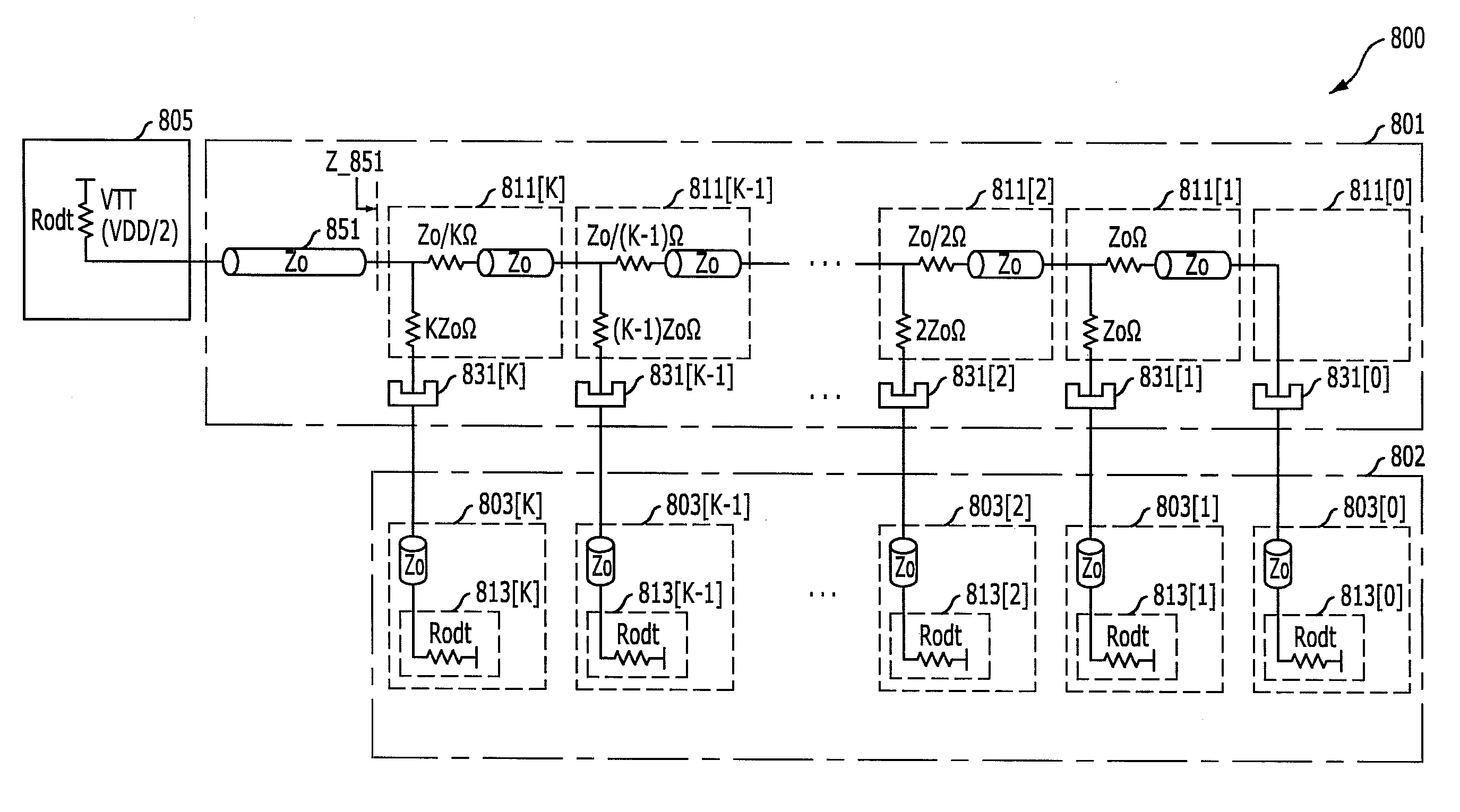
[0014]Embodiments of the present invention are directed to a bi-directional multi-drop bus system which is capable to eliminate the reflected wave causing the ISI, and a memory module and a memory system using the bi-directional multi-drop bus system.

Problems solved by technology

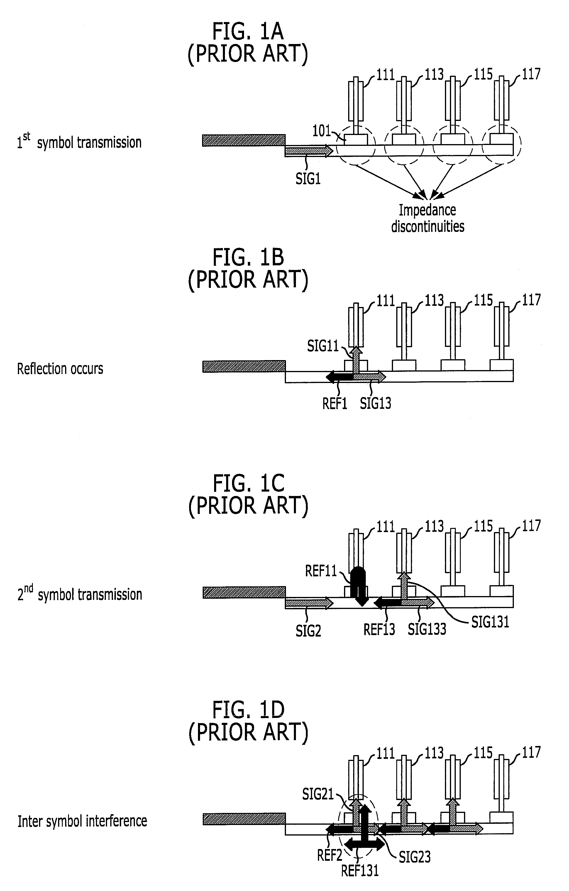
The conventional memory systems employing the SSTL have the problem of the reflected wave induced by the impedance mismatch in the stub.
The reflected wave causing the ISI can seriously damage the signal integrity and, thus, it is impossible to implement the memory systems of the large bandwidth, e.g., greater than 2 Gbps.
Therefore, the conventional SSTL may not be applicable for next generation memory systems which are expected for large bandwidth requirement, e.g., 3.2 Gbps or 6.4 Gbps.
However, the FB-DIMM technique introduces the latency to the memory request and requires additional power consumption for the buffering operation.
For this reason, it is difficult to apply the suggested method to the memory interface channel.

Method used


Image

  • Bi-directional multi-drop bus memory system
  • Bi-directional multi-drop bus memory system
  • Bi-directional multi-drop bus memory system

Examples


Embodiment Construction

[0038]Other objects and advantages of the present invention can be understood by the following description, and become apparent with reference to the embodiments of the present invention.

[0039]FIG. 4 is a schematic diagram describing an equivalent load of a transmission line.

[0040]The equivalent load ZTL1 loaded at a first terminal of a first transmission line TL1 is constituted with resistor loads AΩ and CΩ, which are physical elements, whose second terminals are coupled to the second terminal of the first transmission line TL1, and characteristic impedances DΩ and BΩ of second and third transmission lines TL2 and TL3 whose second terminals are coupled to first terminals of the resistor loads AΩ and CΩ. Because first terminals of the second and third transmission lines TL2 and TL3 are not seen at the first terminal of the first transmission line TL1, the equivalent load ZTL1 loaded at the first terminal of the first transmission line TL1 becomes (A+B)∥(C+D).

[0041]FIG. 5 is a schema...


PUM


Abstract

A bus system includes a plurality of stubs; a plurality of connectors, each of which is serially coupled between a corresponding one of the stubs and a corresponding one of memory modules; a plurality of first serial loads, each of which is serially coupled to a corresponding one of the connectors; and a plurality of second serial loads, each of which is serially coupled to characteristic impedance of a transmission line of a corresponding one of the stubs, wherein the first and the second serial loads are determined to be impedance matched at each transmission line terminal of the stubs.

Description

CROSS-REFERENCE TO RELATED APPLICATION[0001]The present invention claims priority of Korean patent application number 10-2008-0055220, filed on Jun. 12, 2008, the disclosure of which is incorporated herein by reference in its entirety.BACKGROUND OF THE INVENTION[0002]The present invention relates to a bi-directional multi-drop bus system, and a memory module and a memory system using the bi-directional multi-drop bus system.[0003]As the semiconductor fabrication method and the circuit design technique have improved, the bandwidth of the dynamic random access memory (DRAM) has been considerably increased and the data transmission method also has been continuously improved. The increase of the bandwidth influences the direct effect to the operation speed of the input / output (I / O) interface circuit. The operation speed of the I / O interface circuit is determined by the signal integrity of the data channel and the timing margin of the I / O interface circuit.[0004]On the basis of the trans...

Claims


Application Information

Patent Timeline
IPC IPC(8): G06F13/00
CPCG06F13/4086G11C7/1048G11C11/4093G11C11/4096H03K19/017545
Inventor JEONG, DEOG-KYOONKIM, SUHWANSHIN, WOO-YEOLLIM, DONG-HYUKOH, IC-SU
Owner SK HYNIX INC
Learn More