Ad hoc flash memory reference cells

a flash memory and reference cell technology, applied in the field of flash memories, can solve the problems of increasing the size of flash dies, changing the threshold voltage of cells with the time, and the cost of flash silicon substrates

Active Publication Date: 2009-12-24
SANDISK TECH LLC
View PDF9 Cites 19 Cited by
  • Summary
  • Abstract
  • Description
  • Claims
  • Application Information

AI Technical Summary

Problems solved by technology

One of the most disturbing issues in operation of Flash memories is the changing of cells' threshold voltage with the time, due to leakage of charge from the cells' floating gates.
Excess data retention shift may result in errors when reading data from a flash memory, if reading reference voltage levels have not been adjusted in accordance with this shift.
Adding such a significant number of cells to a flash memory page obviously increases the flash die size and, therefore, the cost of the flash silicon substrate.

Method used


Image

  • Ad hoc flash memory reference cells
  • Ad hoc flash memory reference cells
  • Ad hoc flash memory reference cells

Examples


Embodiment Construction

[0032]The principles and operation of a flash memory according to the present invention may be better understood with reference to the drawings and the accompanying description.

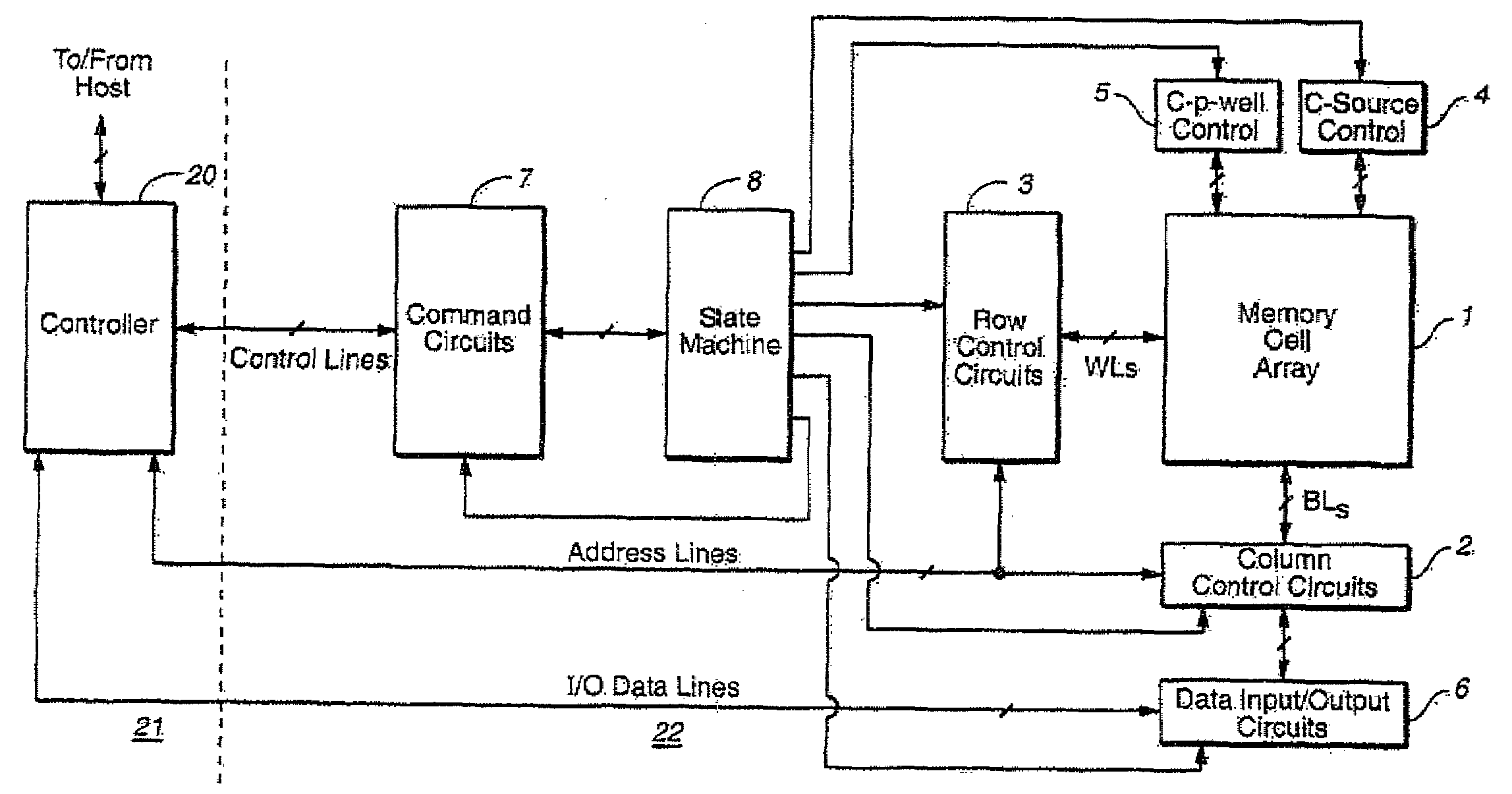
[0033]Referring now to the drawings, FIG. 1 is a high-level schematic block diagram of a flash memory device. A memory cell array 1 including a plurality of memory cells M arranged in a matrix is controlled by a column control circuit 2, a row control circuit 3, a c-source control circuit 4 and a c-p-well control circuit 5. Column control circuit 2 is connected to bit lines (BL) of memory cell array 1 for reading data stored in the memory cells (M), for determining a state of the memory cells (M) during a writing operation, and for controlling potential levels of the bit lines (BL) to promote the writing or to inhibit the writing. Row control circuit 3 is connected to word lines (WL) to select one of the word lines (WL), to apply read voltages, to apply writing voltages combined with the bit line potential le...


PUM


Abstract

In a nonvolatile memory, that includes cells organized in a plurality of bit lines and a plurality of word lines, user data are stored in respective portions of each of two of the word lines. Control information is stored in a cell that is common to one of the bit lines and one of the two word lines. A cell that is common to the bit line and the other word line is used as a reference cell. A flash memory, that includes a plurality of primary cells and a plurality of spare cells, is interrogated to determine which spare cells have been used to replace respective primary cells. At least some of the other spare cells are used as reference cells.

Description

[0001]This patent application claims the benefit of U.S. Provisional Patent Application No. 61 / 074,705, filed Jun. 23, 2008FIELD AND BACKGROUND OF THE INVENTION[0002]The present invention relates to flash memories and, more particularly, to the use, as reference cells, of flash memory cells not initially intended to be used for that purpose.[0003]Flash memories are structured as rectangular arrays of memory cells. The cells are arranged in orthogonal bit lines and word lines. One or more bits of data are written to each cell by injecting sufficient electrical charge into a floating gate of the cell to place the cell's threshold voltage within a range of threshold voltages that represents the value of that bit or of those bits. A flash memory cell is read by comparing its threshold voltage to reference voltages that mark the boundaries between threshold voltage ranges. In the case of a NOR flash memory, the cells may be written and read individually. In the case of a NAND flash memor...

Claims


Application Information

Patent Timeline
Patent Type & Authority Applications(United States)
IPC IPC(8): G06F12/02G06F11/10
CPCG11C16/28G06F12/0246G11C16/3495G11C16/349G11C16/08G11C16/10
Inventor MURIN, MARKSHARON, ERAN
Owner SANDISK TECH LLC
Why Eureka
Try Eureka