
Display device, display device manufacturing method and display method

a display device and manufacturing method technology, applied in the manufacture of electrode systems, electric discharge tubes/lamps, discharge tubes luminescnet screens, etc., can solve the problems of complex structure of organic el panels, fixed images cannot be displayed in the entire display section, and the display quality of displayed images is not the sam

Inactive Publication Date: 2009-12-31
SEIKO EPSON CORP
View PDF4 Cites 14 Cited by
  • Summary
  • Abstract
  • Description
  • Claims
  • Application Information

AI Technical Summary

Benefits of technology

The invention provides a display device with improved image quality and reduced display quality degradation. The display device includes a plurality of pixels arranged in a matrix and a counter electrode. The pixels are arranged in two directions intersecting each other. A first power supply line electrically connects the first direction pixel electrodes, a second power supply line electrically connects the second direction pixel electrodes. The display device can display different images in different unit pixel areas, resulting in almost the same display area for the different images. The display device also includes an insulating layer with light-shielding properties to prevent leak of light. The pixels have an organic layer including a first electrode, a second electrode, and a light-emitting layer sandwiched between the first electrode and the second electrode to emit light. The pixels are classified into pixels emitting light and pixels not emitting light based on the one image in the respective unit pixel areas. The pixels emitting light have a color determined in accordance with the one image in the respective unit pixel areas. The invention provides a display device with improved image quality and reduced display quality degradation.

Problems solved by technology

In addition, it is necessary to control the switching operation of the driving element for each pixel and thus the structure of the organic EL panel is complicated.
Further, the respective fixed images cannot be displayed in the entire display section.
As a result, there is a disadvantage in that display qualities of the displayed images are not the same depending on the light-emitting patterns.

Method used


Image

  • Display device, display device manufacturing method and display method
  • Display device, display device manufacturing method and display method
  • Display device, display device manufacturing method and display method

Examples


first modified example

[0083]In the above embodiments, it has been described that the two images (images A and B) are displayed in the display range. However, the invention is not limited to this and a larger number of images may be displayed. For example, display of three images (images A, B and C) will be described with reference to FIG. 8 and display of four images (images A, B, C and D) will be described with reference to FIG. 9.

(Display of Three Images)

[0084]FIG. 8 is a schematic diagram illustrating a portion of a wiring state on a substrate P. Also in this modified example, similarly to the above embodiments, anodes for respective pixels are formed to be divided into anodes 10, 20 and 30 so that one unit pixel area is formed of four pixels (not shown). In addition, the anodes are arranged in a repeated sequence of the anode 10, the anode 20 and the anode 30 in an X direction and in a repeated sequence of the anode 10, the anode 30 and the anode 20 in a Y direction. The anodes 10, 20 and 30 are elec...

second modified example

[0093]In the above embodiments, the distribution density of the unit pixel areas belonging to the respective images is almost the same in the plural images displayed in the display range. However, the invention is not limited to this. When the number of images displayed in the display range is three or more, the distribution densities of the unit pixel areas belonging to the respective images may be different from each other. In this manner, for example, when the plural images are displayed in the display range, the unit pixel areas belonging to the respective images can be arranged in accordance with the distribution densities of the unit pixel areas necessary for visually confirming the display contents of the images.

[0094]An example of this modified example will be described using FIG. 10. FIG. 10 is a schematic diagram illustrating a portion of a wiring state on a substrate P. Similarly to FIG. 8, the case in which three images are displayed in a display range is illustrated. Al...

third modified example

[0097]In the above embodiments, it has been described that the color of the light emitted from the light-emitting layer formed for each pixel is white. However, the color is not limited to this. For example, in order to display a color image in the display range, the organic EL element formed for each pixel emitting light may be formed to emit light of red (R), green (G) or blue (B).

[0098]An example of this modified example will be described using FIG. 11. FIG. 11 is a schematic diagram illustrating the case in which two images are displayed in a display range. In this modified example, anodes are formed to be divided so that one unit pixel area is formed of the total nine pixels of three pixels in an X direction×three pixels in a Y direction. In addition, anodes 10 and 20 formed to be divided so that an image A which is one of the two images is displayed by the anodes 10 shown by the full line in the drawing and an image B which is the other of the two images is displayed by the an...


PUM


Abstract

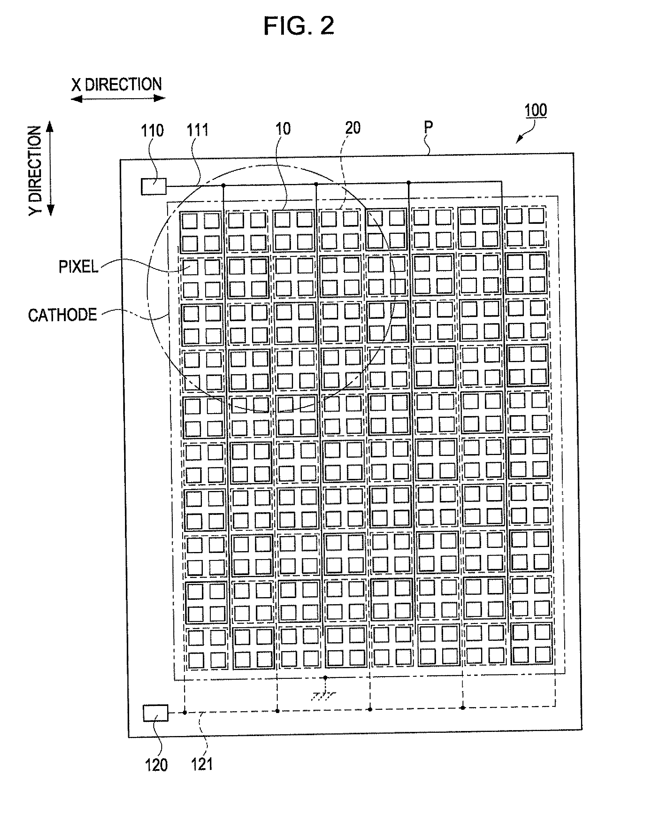
A display device includes: a plurality of first pixel electrodes which are arranged in a first direction and a second direction intersecting the first direction; a plurality of second pixel electrodes which are arranged in the first and second directions; a counter electrode which is formed to be opposed to the plurality of first pixel electrodes and the plurality of second pixel electrodes; a first power supply line which electrically connects the plurality of first pixel electrodes; and a second power supply line which electrically connects the plurality of second pixel electrodes. One or more pixels are formed to correspond to the respective pixel electrodes of the plurality of first pixel electrodes and the plurality of second pixel electrodes. A light-emitting layer made of an organic light-emitting material or an insulating layer made of an organic compound is disposed between a first electrode which is one of the plurality of first pixel electrodes and the counter electrode and between a second electrode which is one of the plurality of second pixel electrodes and the counter electrode. Power is supplied to the plurality of first pixel electrodes via the first power supply line upon displaying a first image and power is supplied to the plurality of second pixel electrodes via the second power supply line upon displaying a second image.

Description

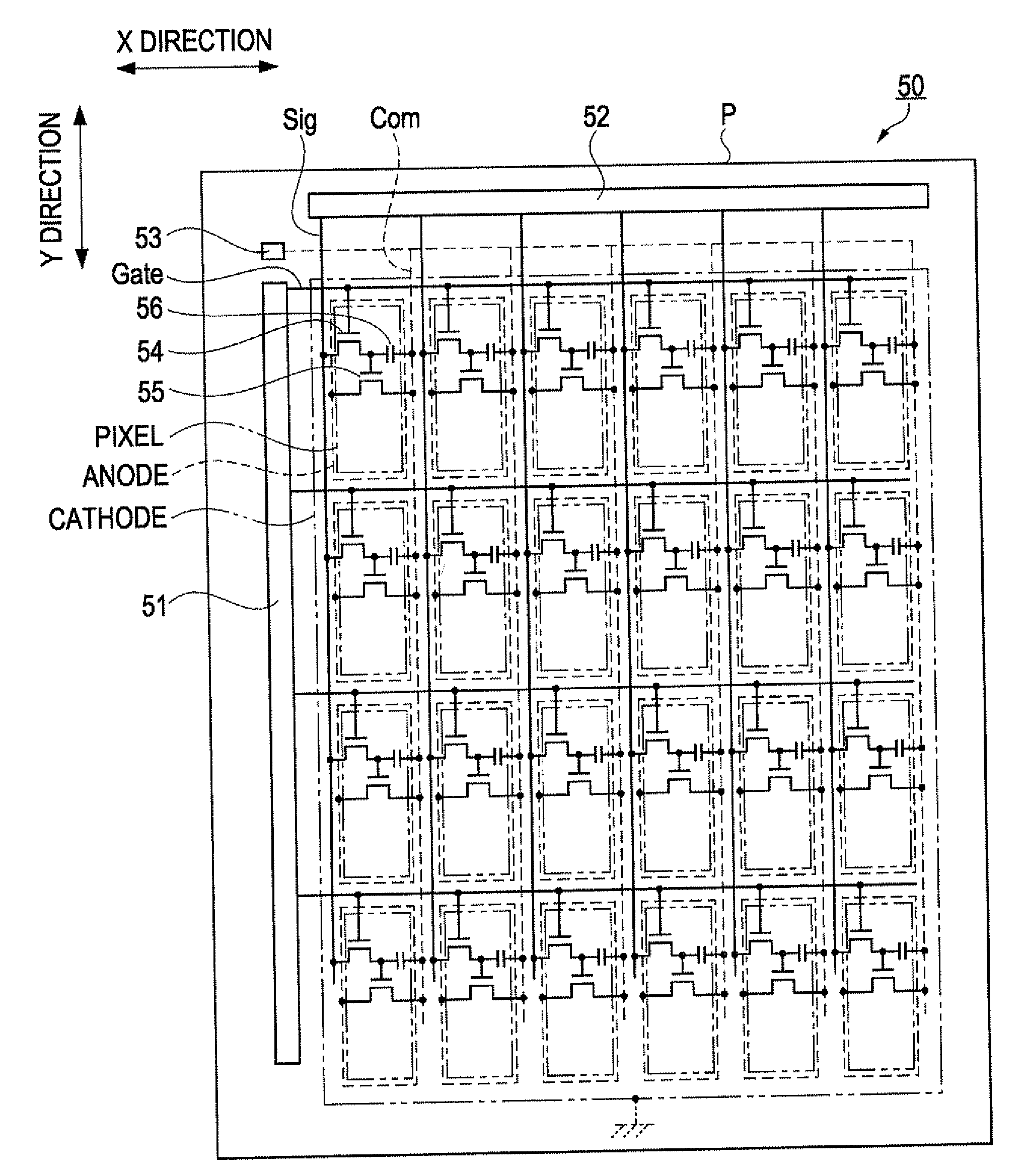
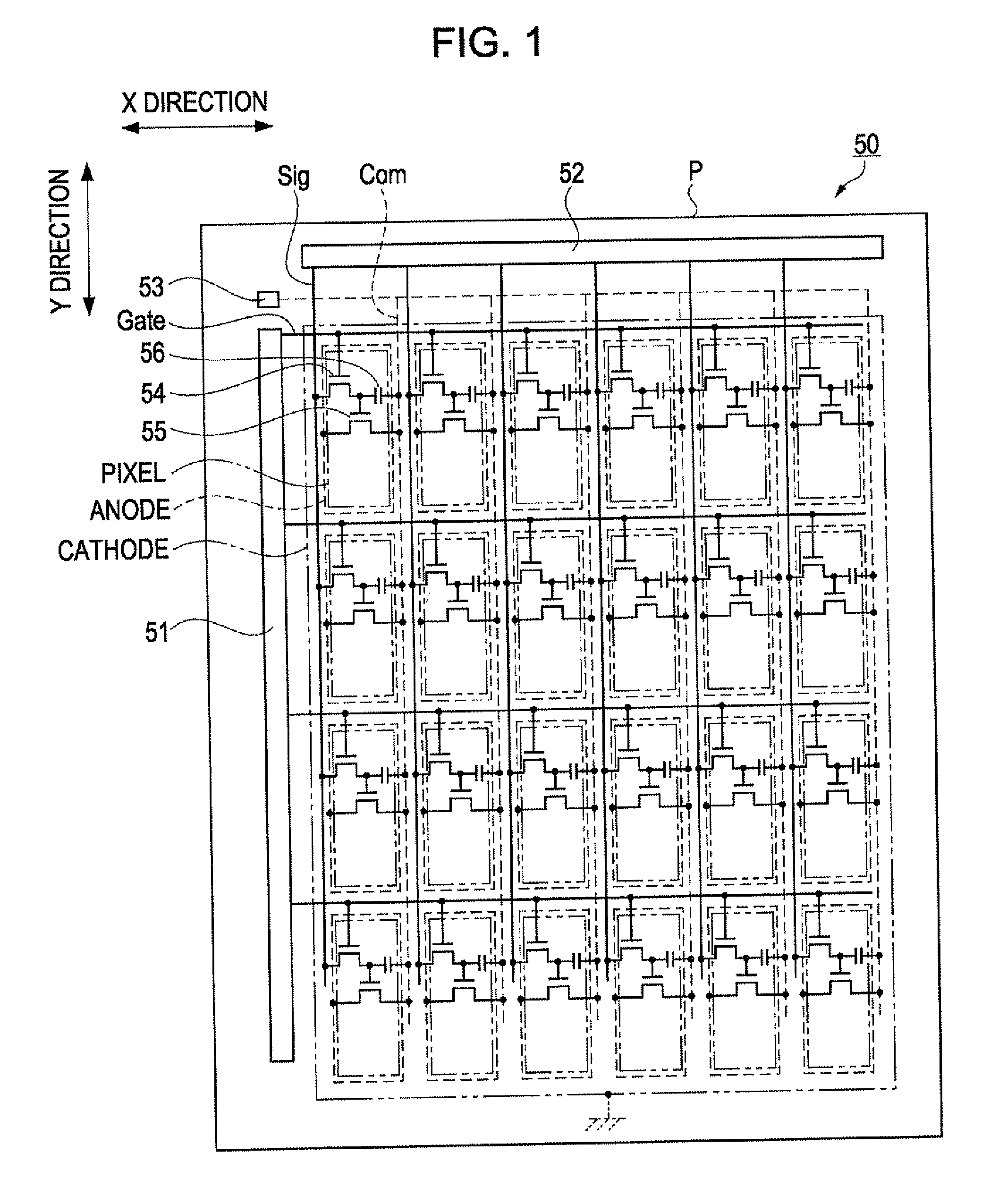
BACKGROUND[0001]1. Technical Field[0002]The present invention relates to a display device, a display device manufacturing method and a display method.[0003]2. Related Art[0004]In recent years, a large number of display devices using, as display elements, electroluminescent elements (EL elements) which are thin spontaneous light-emitting elements have been used. The EL elements have a structure in which plural functional layers including at least a light-emitting layer made of a light-emitting material are formed between an anode as a pixel electrode and a cathode as a counter electrode. A voltage is applied between the anode and the cathode to flow a predetermined current to the functional layers and thus the light-emitting layer emit light and the light having desired brightness is emitted. Particularly, organic EL panels which have, as pixels, organic EL elements made using an organic material as a light-emitting material and in which the pixels are arranged in a matrix to form an...

Claims


Application Information

Patent Timeline
Patent Type & Authority Applications(United States)
IPC IPC(8): H01J1/62H01J1/53H01J9/20
CPCH01L27/3211H01L51/0005H01L27/3288H01L27/3239H10K59/221H10K59/35H10K59/179H10K71/135
Inventor YANAGIHARA, HIROKAZU
Owner SEIKO EPSON CORP
Learn More