Smi memory read data capture margin characterization circuits and methods
a data capture and memory read technology, applied in the field of characterization of asic performance margins, can solve problems such as unsatisfactory strobes and data in a system
- Summary
- Abstract
- Description
- Claims
- Application Information
AI Technical Summary
Benefits of technology
Problems solved by technology
Method used
Image

Examples
Embodiment Construction
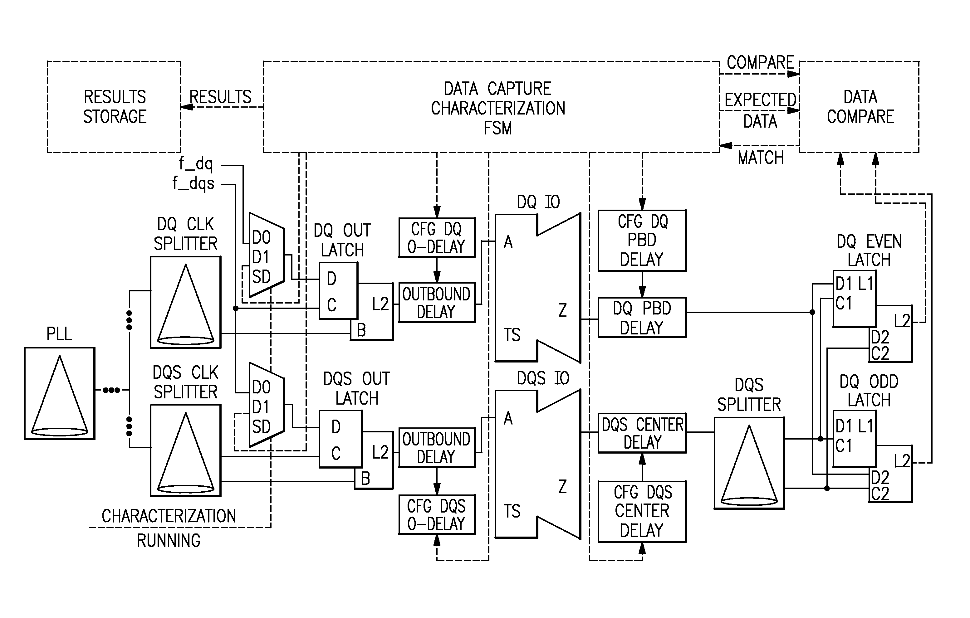
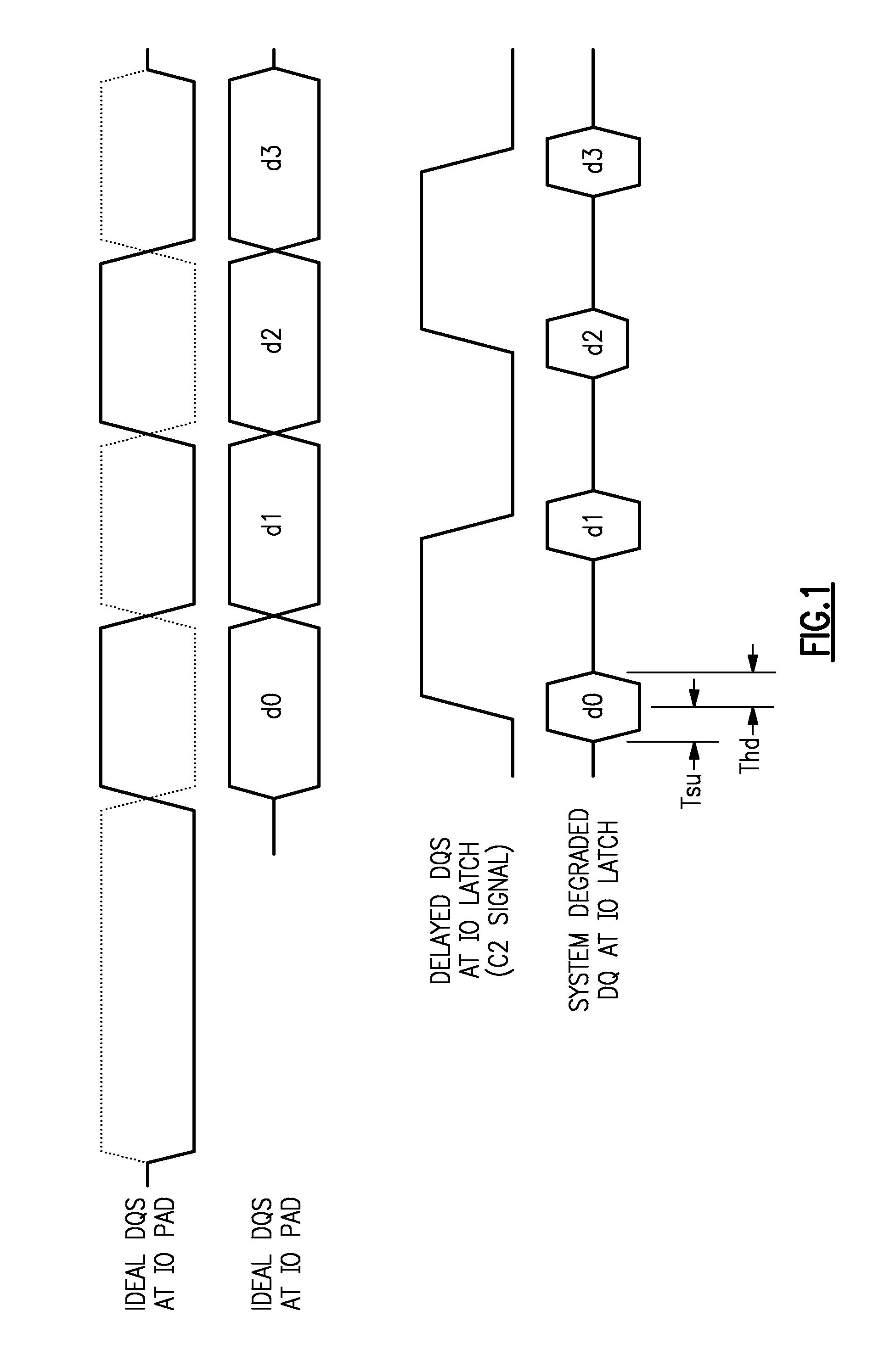
[0026]Turning now to the drawings in greater detail, FIG. 1 illustrates the timing diagrams of SDRAM memory read operation in a timing test. FIG. 1 shows a burst of four data shots of a memory read operation, d0, d1, d2, and d3. The SDRAM launches strobe (DQS) coincident with data (DQ). The SMI must delay the strobe ½ bit-time in order to center it within the data window and capture each data transfer with an edge of the strobe. The top portion of FIG. 1 shows an ideal arrival of strobe and data at the 10 pad. The bottom portion of FIG. 1 shows strobe, delayed by ½ bit-time, as it would arrive at the 10 latch. The data pulse is shown as it would be degraded for the timing test. For a typical SMI chip specification, ⅔ of the data window would be allocated to the SDRAM and off-chip timing degradation effects (e.g. wire length mismatches, coupled noise), so the chip internal circuitry would be allowed to degrade the pulse by no more than another ⅓. Chip timing analysis and hardware cha...
PUM
 Abstract
Description
Claims
Application Information
 - Generate Ideas
- Intellectual Property
- Life Sciences
- Materials
- Tech Scout
- Unparalleled Data Quality
- Higher Quality Content
- 60% Fewer Hallucinations
Browse by: Latest US Patents, China's latest patents, Technical Efficacy Thesaurus, Application Domain, Technology Topic, Popular Technical Reports.
© 2025 PatSnap. All rights reserved.Legal|Privacy policy|Modern Slavery Act Transparency Statement|Sitemap|About US| Contact US: help@patsnap.com