Chip on film trace routing method for electrical magnetic interference reduction

a technology of electrical magnetic interference and trace routing, which is applied in the direction of cross-talk/noise/interference reduction, line-transmission details, and semiconductor/solid-state device details, etc., can solve the problems of reducing the overall affecting the performance of electronic devices, and affecting the effect of emi reduction

Inactive Publication Date: 2009-12-31
HIMAX TECH LTD
View PDF7 Cites 7 Cited by
  • Summary
  • Abstract
  • Description
  • Claims
  • Application Information

AI Technical Summary

Benefits of technology

[0005]It is therefore one of the objectives of the present invention to provide a COF trace routing method for reducing the EMI effect, in order to solve the above-mentioned problem.

Problems solved by technology

However, an undesirable EMI easily occurs when the components of the electronic devices manufactured by the COF packaging technique transmit high-speed signals (usually differential signals).
Thus, the overall performance of the electronic devices is degraded due to the EMI effects.
For this reason, how to suppress EMI effect has become a major issue for the COF packaging technique.

Method used


Image

  • Chip on film trace routing method for electrical magnetic interference reduction
  • Chip on film trace routing method for electrical magnetic interference reduction

Examples


Embodiment Construction

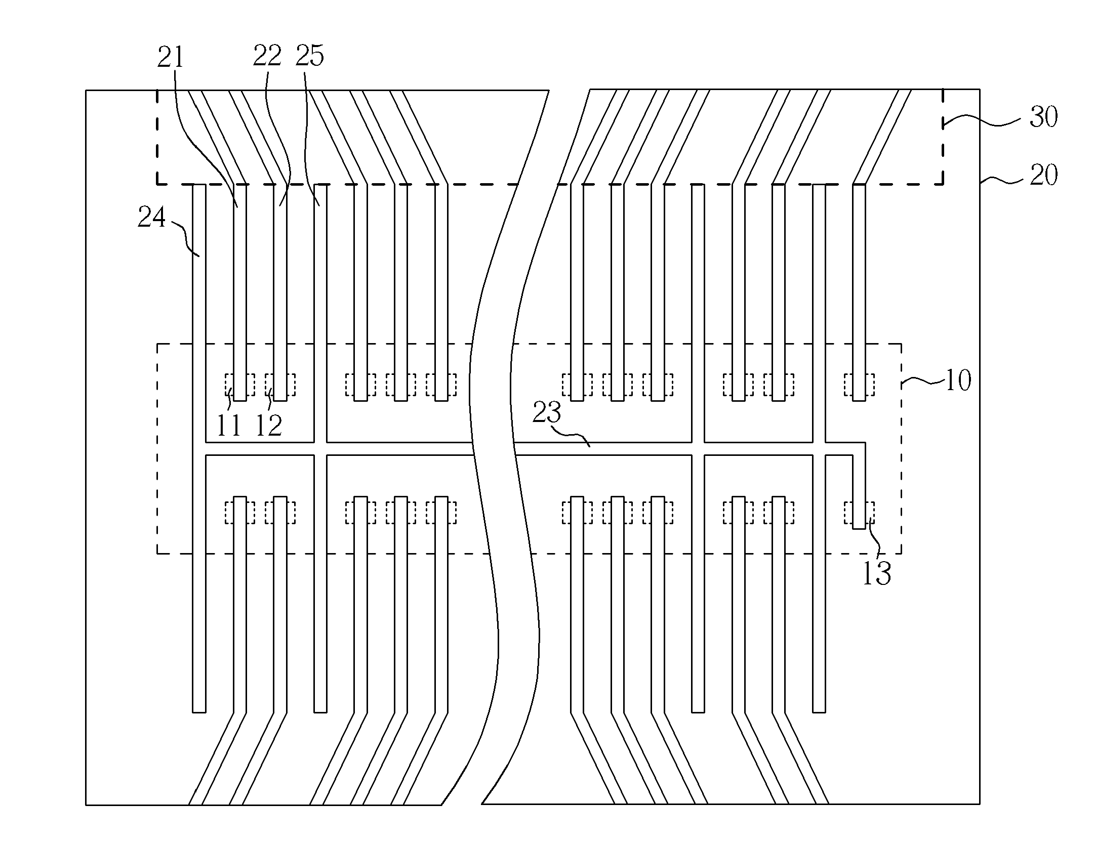
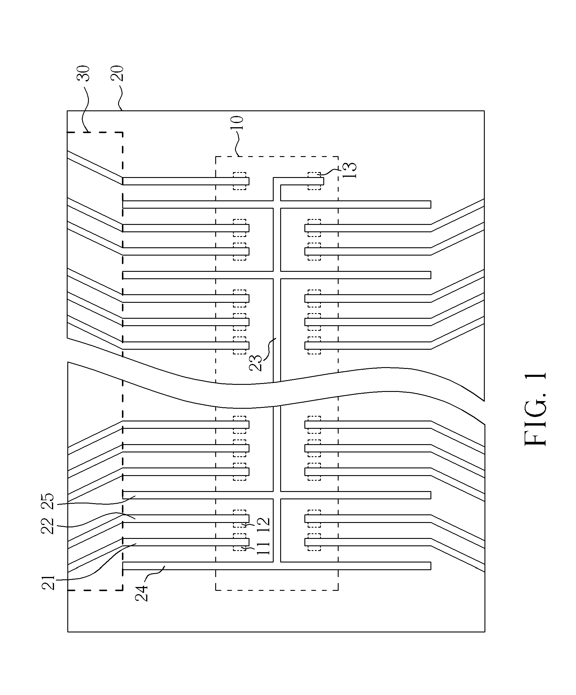
[0010]Please refer to FIG. 1. FIG. 1 is a simplified plane view illustrating a chip on film (COF) structure 100 according to an embodiment of the present invention. The COF structure 100 comprises a chip 10, such as a driver IC, and a flexible circuit board 20, such as a flexible printed circuit (FPC) board. The chip 10 has a plurality of pads, including a first signal pad 11, a second signal pad 12 and a ground pad 13. The flexible circuit board 20 has a plurality of wiring traces, including a first signal trace 21, a second signal trace 22, a central ground trace 23, a first ground trace 24 and a second ground trace 25. Further description of the COF structure 100 is detailed as follows; however, this description is merely for greater clarity of understanding, and should not be taken as limiting the present invention.

[0011]The first and second signal traces 21, 22 are immediately adjacent to one another, and are disposed between the first ground trace 24 and the second ground trac...


PUM


Abstract

A chip on film (COF) trace routing method for EMI reduction includes: providing a flexible circuit board; mounting a chip that has a first signal pad, a second signal pad and a ground pad on the flexible circuit board; and forming a first signal trace, a second signal trace, a first ground trace and a second ground trace on the flexible circuit board. The first signal trace and the second signal trace are electrically connected to the first signal pad and the second signal pad respectively. The first ground trace and the second ground trace are both electrically connected to the ground pad. The first signal trace and the second signal trace are disposed between the first ground trace and the second ground trace. The first ground trace and the second ground trace are immediately adjacent to the first signal trace and the second signal trace respectively.

Description

BACKGROUND OF THE INVENTION [0001]1. Field of the Invention[0002]The present invention relates to a chip on film (COF), and more particularly, to a COF trace routing method for electrical magnetic interference (EMI) reduction.[0003]2. Description of the Prior Art[0004]COF, a packaging technique that requires less space for the I / O interconnections, has been widely used to manufacture components of electronic devices, such as driver ICs for liquid crystal displays (LCD). However, an undesirable EMI easily occurs when the components of the electronic devices manufactured by the COF packaging technique transmit high-speed signals (usually differential signals). Thus, the overall performance of the electronic devices is degraded due to the EMI effects. For this reason, how to suppress EMI effect has become a major issue for the COF packaging technique.SUMMARY OF THE INVENTION [0005]It is therefore one of the objectives of the present invention to provide a COF trace routing method for r...

Claims


Application Information

Patent Timeline
Patent Type & Authority Applications(United States)
IPC IPC(8): H04B3/28H05K9/00
CPCH01L23/49572H01L23/552H05K1/0219H05K1/111H05K1/189H01L2924/0002H05K2201/10674H01L2924/00
Inventor CHEN, PENG-CHILIN, CHIH-HSIANG
Owner HIMAX TECH LTD
Why Eureka
Try Eureka