Printed circuit board assembly and method for preventing EMI of crystal oscillator thereof

Inactive Publication Date: 2007-01-04
BENQ CORP
View PDF5 Cites 2 Cited by
  • Summary
  • Abstract
  • Description
  • Claims
  • Application Information

AI Technical Summary

Benefits of technology

[0008] It is therefore an object of the invention to provide a method promptly and correctly enabling the shell of the crystal oscillator to be connected to the ground layer of the PCBA without using manual soldering process, thereby reducing the EMI effect of the crystal oscillator.
[0009] The invention achieves the above-identified object by providing a PCBA including a crystal oscillator and a print circuit board (PCB). The crystal oscillator includes a body and a shell. The shell covers the body. The PCB includes an inserting area and at least a plated hole. The inserting area is used for receiving the body. The inserting area disposed on one side of the PCBA is used for receiving the crystal oscillator. The inserting area is designed as a ground bare copper and includes a pre-soldering area. The plated hole is disposed on the pre-soldering area. The inner surface of the plated hole is electroplated with a coating of conductive metal for guiding the solder. The ground layer is electrically connected to the shell via the solder for enabling the shell to be connected to the ground layer, so that the EMI effect is reduced. Besides, the plated hole is able to be electrically connected to other ground layers of the PCBA, so that the grounded area of the shell is increased and the shielding effect is enhanced.

Problems solved by technology

However, crystal oscillators, which often generate high oscillation frequency during oscillation, would easily result in electrical magnetic interference (EMI) effect.
If the EMI effect is too large, the efficiency of the PCBA or the entire system would be affected.
However, the wave soldering process would make the crystal oscillator 103 crippled, affecting the contact between the shell of the crystal oscillator 103 and the ground bare copper of the inserting area and deteriorating the shielding effect.
However, the additional manual soldering process is both labor and time consuming.
Besides, the components surrounding the crystal oscillator could be damaged due to carelessness in soldering process.

Method used


Image

  • Printed circuit board assembly and method for preventing EMI of crystal oscillator thereof
  • Printed circuit board assembly and method for preventing EMI of crystal oscillator thereof
  • Printed circuit board assembly and method for preventing EMI of crystal oscillator thereof

Examples


first embodiment

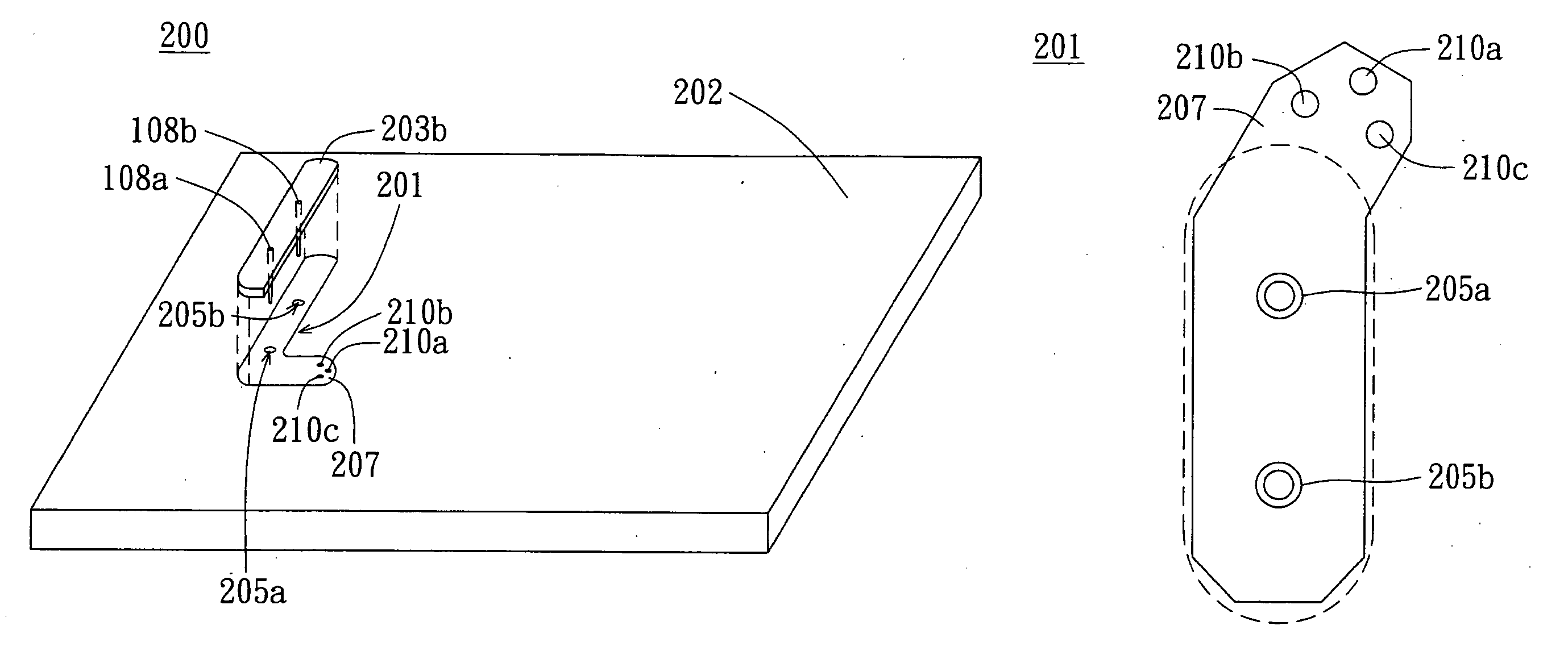
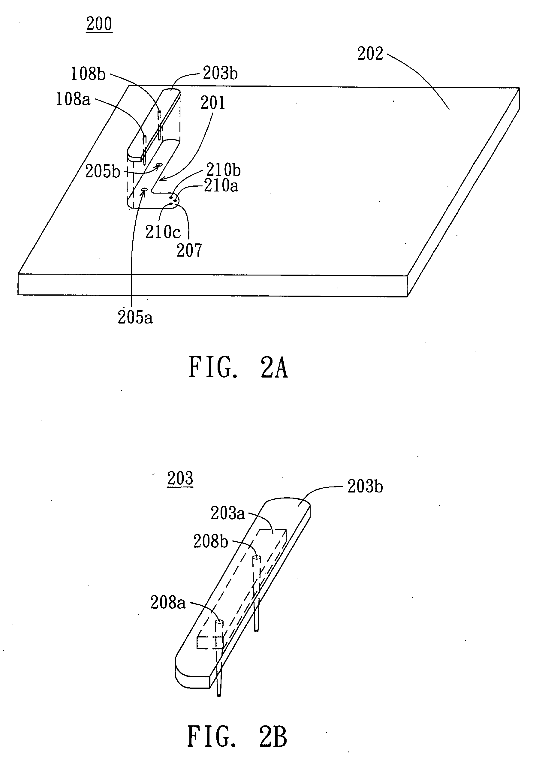
[0021] Referring to FIG. 2A, FIG. 2B and FIG. 2C at the same time. FIG. 2A is a diagram showing the relationship between a crystal oscillator and a PCBA according to the first embodiment of the invention. FIG. 2B is a 3-D diagram of a crystal oscillator. FIG. 2C is a top view of an inserting area and a pre-soldering area. The PCBA 200 includes a crystal oscillator 203 and a PCB 202 (the print circuit board, PCB). The PCB 202 reserves an inserting area 201. The inserting area 201 has a pre-soldering area 207. The pre-soldering area 207 has several plated holes 210a-210c. The pre-soldering area 207 includes metal, and preferably the metal is bare copper. The inserting area 201 has two holes 205a and 205b, and the inserting area 201 is disposed on one side of the PCBA 200. The crystal oscillator 203 has the body 203a and the shell 203b. The shell 203b covers the body 203a for protecting the electronic components inside the body 203a. Meanwhile, the crystal oscillator 203 further includ...

second embodiment

[0023] In the aforementioned embodiment, for the convenience of checking the reliability that the plated hole electrically connects the shell and the ground layer via the solder, the plated hole is disposed close to the surface of the shell. Under stable and reliable conditions of technology, the invention can be achieved by another embodiment.

[0024] Referring to both FIG. 3A and FIG. 3B. FIG. 3A is a top view of plated holes and a crystal oscillator according to the second embodiment of the invention, and FIG. 3B is a cross-sectional view of the crystal oscillator of FIG. 3A. The plated holes 310a-310d are disposed under the crystal oscillator 303, thus omitting the pre-soldering area and reducing the area of the PCBA. That is, the plated holes 310a-310d are directly connected to each ground layer of the PCBA 300. For example, the plated holes 310a-310d are connected to the ground layer 312. In the present embodiment, the closer to the shell 303b the plated holes 310a-310d are dis...


PUM


Abstract

A printed circuit board Assembly (PCBA), including at least one crystal oscillator and a printed circuit board (PCB), is provided. The crystal oscillator includes a body and a shell. The shell covers the body. The PCB includes at least one inserting area and at least one plated hole. The inserting area is used for receiving the body. The plated hole is disposed on the inserting area. When the PCBA is under wave soldering process, the solder is drawn from one side of the PCBA to another side via the plated hole for enabling the shell to be electrically connected to the bare copper of the inserting area via the solder. Consequently, the shell has an even better shielding effect, and the EMI effect is reduced.

Description

[0001] This application claims the benefit of Taiwan application Serial No. 94122396, filed Jul. 1, 2005, the subject matter of which is incorporated herein by reference. BACKGROUND OF THE INVENTION [0002] 1. Field of the Invention [0003] The invention relates in general to a printed circuit board assembly (PCBA) and a manufacturing method thereof, and more particularly to a PCBA capable of preventing EMI effect of a crystal oscillator and a manufacturing method thereof. [0004] 2. Description of the Related Art [0005] Crystal oscillators, which have now been widely applied in various systems, are aimed at providing a standard of reference for the oscillation frequency of the system. However, crystal oscillators, which often generate high oscillation frequency during oscillation, would easily result in electrical magnetic interference (EMI) effect. If the EMI effect is too large, the efficiency of the PCBA or the entire system would be affected. A method for preventing EMI effect of ...

Claims


Application Information

Patent Timeline
IPC IPC(8): H05K1/11
CPCH05K1/0243H05K3/3447H05K2203/0455H05K2201/10075H05K2201/10969H05K3/3468
Inventor CHAI, QING-LI
Owner BENQ CORP
Why Eureka
Try Eureka