A kind of soft driving method and circuit of power mosfet

A soft drive and MOS tube technology, applied in the direction of output power conversion devices, electrical components, etc., can solve the problems of non-MOSFET drive circuits, large conduction loss, and poor EMI performance, so as to reduce EMI effects and reduce conduction Loss, the effect of reducing EMI

Active Publication Date: 2018-06-26
MORNSUN GUANGZHOU SCI & TECH
View PDF6 Cites 0 Cited by
  • Summary
  • Abstract
  • Description
  • Claims
  • Application Information

AI Technical Summary

Problems solved by technology

like Figure 4a , Figure 4b and Figure 5a , Figure 5b As shown, it is the simulation curve of the gate drive process of the gate drive circuit of an existing switching power supply flyback converter working under CCM and DCM, t0-t1 is the time to reach the threshold voltage, t1-t2 bits enter The time of the Miller platform, t2-t3 is the time of the Miller platform, and t3-t4 is the time of exiting the Miller platform. It can be seen that the time period t3-t4 for exiting the Miller platform after the MOSFET is fully turned on is 150ns and 180ns. This period of time is too long, resulting in a large conduction loss (conduction loss refers to the loss caused by the voltage drop generated by the load current (ie, drain-source current) IDSon(t) on the on-resistance RDSon after the MOSFET is fully turned on), Especially after the MOSFET working under CCM is fully turned on, IDS does not start to rise from 0A, but a very large current. If the time t3~t4 of exiting the Miller platform is very long, the conduction loss will be very large, from In terms of efficiency, it can be seen that the existing technology is not a very good MOSFET drive circuit
[0010] Generally, in order to reduce the conduction loss, the current technology usually increases the charging current for charging the MOSFET capacitor, speeds up the Vgs voltage rise rate, and then reduces the time t3~t4 for exiting the Miller platform. Although this can reduce the conduction The purpose of loss, but also reduces the Miller platform and the total time before it t0 ~ t3, EMI performance becomes worse; or in order to achieve good EMI performance, a compromise between conduction loss and EMI performance, but conduction loss It is still relatively large, nothing more than the existing technology is not a very good MOSFET drive circuit

Method used


Image

  • A kind of soft driving method and circuit of power mosfet
  • A kind of soft driving method and circuit of power mosfet
  • A kind of soft driving method and circuit of power mosfet

Examples


Embodiment 1

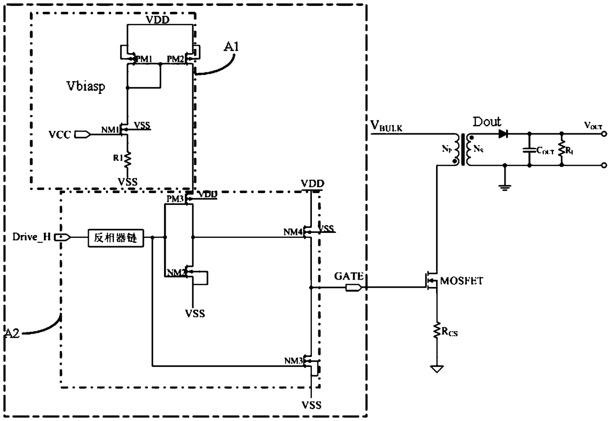
[0046] Such as Figure 6 As shown, it is a power MOSFET soft driving circuit diagram according to Embodiment 1 of the present invention. A soft drive circuit for power MOSFETs, comprising: a current bias unit A11, a drive chain unit A12 and a positive feedback current generation unit A13.

[0047] Current bias unit A11 and drive chain unit A12 and background technology figure 2 The circuit shown is the same, and only the number of each component is distinguished by adding 10 in front of it, so it will not be repeated here.

[0048]The positive feedback current generating unit A13 is composed of resistor R102, resistor R103, N-channel MOS transistor NM105, N-channel MOS transistor NM106, N-channel MOS transistor NM107, P-channel MOS transistor PM104, P-channel MOS transistor Tube PM105, P-channel MOS tube PM106, diode D1, logic NOT gate INV101, and logic NOT gate INV102. The first port of the resistor R102, the gate of the N-channel MOS transistor NM107, and the output term...

Embodiment 2

[0051] Such as Figure 9 As shown, it is a power MOSFET soft drive circuit diagram of the second embodiment of the present invention, including: a current bias unit A21, a drive chain unit A22 and a positive feedback current generation unit A23.

[0052] The current bias unit A21 is composed of a current mirror composed of a P-channel MOS transistor PM201, a P-channel MOS transistor PM202, and a P-channel MOS transistor PM203. The input bias current Ibp_40u is connected to the drain of the P-channel MOS transistor PM201 The input bias current Ibp_40u is obtained by mirroring the internal bias current of the chip through the current mirror. The gate and drain of the P-channel MOS transistor PM201, the gate of the P-channel MOS transistor PM202, and the gate of the P-channel MOS transistor The gate of PM203 is connected with the output end of positive feedback current generation unit A23, the source and substrate of P-channel MOS transistor PM201, the source and substrate of P-c...


PUM


Abstract

The invention discloses a soft driving method of a power MOSFET and a corresponding circuit. In a period from when the MOSFET starts to be electrified till a Miller platform is finished, soft driving current I1 is very small, a conduction process of the MOSFET is delayed, and EMI is reduced; when the MOSFET exits from the Miller platform, driving current and positive feedback large current I2 are superposed, the superposed large current is used to charge an MOSFET input capacitor, VGS voltage rises quickly, unnecessary charge consumption is reduced, i.e., conduction loss is reduced, and efficiency is improved; and after the VGS voltage rises to the highest driving voltage, the positive feedback large current I2 quickly reduces to zero. The method and the circuit provided by the invention achieve very good beneficial effects in reduction of an EMI effect, reduction of conduction loss and improvement of efficiency.

Description

technical field [0001] The invention relates to a soft driving method and circuit, in particular to a gate soft driving method and circuit applied to power MOSFETs. Background technique [0002] Driving circuit design is one of the key points in the application of power MOSFETs, and the gate driving process of MOSFETs can be simply understood as the charging and discharging process of the driving power supply to the MOSFET input capacitance. Get the static parameter. However, in practical applications, the parameters of these capacitors are nonlinear functions of temperature and voltage, and affected by the Miller effect, the total dynamic input capacitance will be much larger than the total static capacitance. All of these have brought great difficulties to the accurate analysis of gate drive. But from an application point of view, it is necessary to understand the characteristics of its driving process. [0003] Such as figure 1 As shown, it is the inter-electrode capa...

Claims


Application Information

Patent Timeline
Patent Type & Authority Patents(China)
IPC IPC(8): H02M1/08H02M1/44
Inventor 赵志伟唐盛斌
Owner MORNSUN GUANGZHOU SCI & TECH
Why Eureka
Try Eureka